All GB/s without FLOPS - Nvidia CMP 170HX Review, Performance Lockdown Workaround, Teardown, Watercooling, and Repair
Introduction
In 2021, at the height of cryptocurrency mining, Nvidia released the Nvidia CMP 170HX. Designed as a compute-only card to accelerate Ethereum’s memory-hard Ethash Proof-of-Work mining algorithm with its 1500 GB/s HBM2e memory bus, Nvidia implemented the hardware using the GA100 silicon from their Ampere architecture. Thus, the CMP 170HX is essentially a variant of the all-mighty Nvidia A100, Nvidia’s top-performing datacenter GPU at that time.
Naturally, the existence of the CMP 170HX raised many questions, including its potential in applications beyond mining. Today, following the discontinuation of Ethash, these $5000 GPUs from closed mining farms are sold on second-hand markets for $400-$500 in China. It’s time to answer these questions.
This article contains a basic performance overview, a hardware teardown, a watercooling installation guide, and a repair log.
TL;DR
The Nvidia CMP 170HX is a variant of the Nvidia A100, and has its full memory bandwidth of 1500 GB/s. But benchmarks found that the CMP 170HX’s FP32 FMA/MAD throughput has been throttled by Nvidia to a useless level of 0.39 TFLOPS (390 GFLOPS) - slower than a GPU from 15 years ago or even today’s CPUs. FMA throttling makes it impractical for running any ready-made software due to their usage of an instruction which has been made useless on this card. For FP16 (42 TFLOPS) and non-FMA FP32 compute (6.25 TFLOPS), judging from its FLOPS alone, although artificial throttling did not make them completely useless, but this is merely as fast as a recent-gen low-end GPU similar to an RTX 2060. Only integer performance is relatively uncapped at 12.5 TIOPS (80% of RTX 2080 Ti, 60% of Nvidia A100) for its intended application of Ethereum mining.
But it would be unfair to dismiss this GPU completely for its low FLOPS while ignoring its huge GB/s. Under a very particular set of conditions: When an FP32 workload is extremely limited by memory bandwidth rather than floating-point performance (and when it’s practical to modify such a program to remove FMA usages from source code) - the CMP 170HX can be as fast as a real Nvidia A100 in a suitable FP32 workload thanks to its full 1500 GB/s HBM2e memory bus, thus beating all customer-grade GPUs currently in existence like the RTX 4090 by up to 50% (which “only” has 1 TB/s of memory bandwidth). More impressively, this is done at less than 1% of the price of an Nvidia A100. This situation is true for many memory-bound physics simulations in science and engineering. The same can be said for memory-bound pure-integer workloads (the GPU was made for mining after all).
Unfortunately, while memory-bound physics simulations that scale linearly with memory bandwidth is a huge thing in the field of High-Performance Computing - it’s a niche application in the grand scheme of things. Worse, even if your workload meets this particular set of conditions, removing FMA usages from code can be impractical in many cases - although I’ve demonstrated some possible solutions in Appendix 0 (while also explaining their limitations).
In addition, to prevent the GPU from being used for general compute, Nvidia further restricted its VRAM size to 8 GiB, limited its PCIe bandwidth to PCIe 1.0 x4 at 1 GB/s (upgradable to x16 by hardware modding, but still at PCIe 1.0’s 4 GB/s), and without NV-Link - which means it’s only suitable for a small-to-medium size simulation without the need of frequent PCIe communications to CPUs or to other GPUs (e.g. it’s coded in a way to do on-GPU data reduction). This limited the use case of its high memory bandwidth to all but the simplest simulations, excluding its use in any serious HPC applications with the possible exception of related software development (which was what I purchased this GPU for). Due to firmware signing, bypassing these limitation via VBIOS modding is unlikely.
Due to floating-point throughput lockdown, most stress test tools would report under 75 watts of power consumption - which is highly misleading. With a suitable workload, even an FP32 workload (non-FMA and heavy in memory traffic) can have a power consumption as high as 180 watts using a modified version of FluidX3D. I expect an integer + memory workload can push the power to above 200 watts.
In Appendix 1, the CMP 170HX was dismantled, its circuit board was found to be almost if not fully identical to Nvidia A100 40 GB PCIe version (not 80 GB or SXM versions), demonstrated from the fact that leaked Nvidia A100 circuit schematics were found to match it perfectly and was even successfully used to fix a broken CMP 170HX in Appendix 3. The only obvious difference is that some components are omitted on the circuit board. Owners of the Nvidia A100 who want to perform a modification to their expensive cards may want to practice with an inexpensive CMP 170HX first.
Like most server-grade GPUs, these cards use a passive cooler expected
to be cooled from high-RPM fans on a server chassis, the noise of
these fans is usually unacceptable for workstation use in homes
and offices. Watercooling solutions exist for the Nvidia A100, and
thus also for the CMP 170HX. Ready-made waterblocks allow their use
in workstations at home for silent operations at a cool temperature.
Appendix 3 shows the installation of a Bykski N-TESLA-A100-X-V2
waterblock,
with potential pitfalls and hazards highlighted in the procedures
to prevent future readers from damaging their GPU if they decide to
perform the same modification (I believe currently the only guide
for this Bykski waterblock on the Web).
For people who want to use mining-special GPUs for general compute due their cheap price, a much better alternative is the mining-special AMD Radeon VII (sold as Instinct MI50 - not real MI50s but a weird hybrid between the two), the price is currently $100 in China, with 1 TB/s memory bandwidth, and unlocked FP32 and FP64 performance just like the real MI50, making it possibly the best GPU of all time in terms of price-performance.
Performance Overview
Hardware Specification
The Nvidia CMP 170HX contains 8960 shaders. Without artificial limitations on instruction throughput, these shaders should reach a peak FP32 performance of 25 TFLOPS.
------------------------ Device specifications ------------------------
Device:              NVIDIA Graphics Device
CUDA driver version: 12.20
GPU clock rate:      1410 MHz
Memory clock rate:   729 MHz
Memory bus width:    4096 bits
WarpSize:            32
L2 cache size:       32768 KB
Total global mem:    7961 MB
ECC enabled:         No
Compute Capability:  8.0
Total SPs:           8960 (70 MPs x 128 SPs/MP)
Compute throughput:  25267.20 GFlops (theoretical single precision FMAs)
Memory bandwidth:    1492.99 GB/sec
-----------------------------------------------------------------------
Memory Bandwidth
clpeak shows the Nvidia CMP 170HX has a peak memory bandwidth of 1355 GB/s for
real without any downsizing. Thanks to the use of HBM2e and a wide bus, this is
right now the GPU with the fastest memory that money can buy at an affordable price.
The speed is nearly identical to the Nvidia A100 (HBM2e), and ~1.5x as fast as
the current top customer-grade GPUs, including the Nvidia RTX 4090 (GDDR6X),
AMD Radeon 7900 XTX (GDDR6), or the AMD Radeon VII / Instinct MI50 (HBM2), which
all topped out at “only” 700-800 GB/s with their 1 TB/s memory buses.
Global memory bandwidth (GBPS)
  float   : 1165.79
  float2  : 1269.69
  float4  : 1343.50
  float8  : 1355.40
  float16 : 1350.14
However, this is where all the good news ends.
Floating-Point Performance
FP32 & FP64 with FMA (clpeak, standard version)
To measure the peak floating-point performance of a processor, most benchmarks
use the Multiply-Add operation in the form of a * b + c in their compute
kernels (i.e. inner loop) which is accelerated by the Fused Multiply-Add (FMA)
or Multiply-Add (MAD) instructions in most processors - clpeak is not
an exception.
Unfortunately, tests show heavy performance restrictions on FMA and MAD floating-point operations, with a FP32 FMA speed of 394 GFLOPS and a FP64 FMA speed of 182 GFLOPS. The FP32 FMA performance is 1/100 of today’s high-end GPUs. To put this into perspective, this is not only slower than the Nvidia GTX 280 GPU from 15 years ago - it’s even slower than a 2020s multi-core CPU (> 1 TFLOPS).
This kind of restrictions is often applied to FP64 performance on customer-grade GPUs to prevent their use in computing workloads, but for the CMP 170HX, FP32 basically received the same treatment.
Single-precision compute (GFLOPS)
  float   : 394.77
  float2  : 394.77
  float4  : 394.77
  float8  : 394.77
  float16 : 394.77

No half precision support! Skipped

Double-precision compute (GFLOPS)
  double   : 182.72
  double2  : 182.55
  double4  : 182.19
  double8  : 181.48
  double16 : 180.08
FP32 and FP64 without FMA (clpeak, modified version)
Upon further investigation using a self-written benchmark, I found regular FP32 add or multiply is not restricted by that much. Thus, using a non-standard and patched version of clpeak without the use of FMA instructions entirely, the following results are obtained.
Single-precision compute (GFLOPS)
  float   : 6285.48
  float2  : 6287.64
  float4  : 6294.30
  float8  : 6268.80
  float16 : 6252.80

No half precision support! Skipped

Double-precision compute (GFLOPS)
  double   : 94.98
  double2  : 94.93
  double4  : 94.84
  double8  : 94.65
  double16 : 94.29
Without FMA, the FP32 performance is around 6250 GFLOPS. 6250 GFLOPS is around the speed of a recent low-end desktop GPU such as an RTX 2060, or an old high-end GPU from yesteryear, such as a Titan X (Maxwell).
This is rather low but may still be very acceptable, since many physics simulations for scientific and engineering applications do not benefit from improved core performance in terms of FLOPS, and instead are primarily limited by memory bandwidth.
On the other hand, FP64 performance is now even lower without FMA, at a nearly useless level of 94 GFLOPS. Thus, one may argue that it’s useless for HPC uses. However, the use of FP64 is not always required depending on the research subject. For many Partial Differential Equation solvers for physics simulation, FP32 is in fact the standard. First, the meshing and discretization errors are often much larger sources of error, not to mention that FP64 would slow down these already memory-bound simulations even further. Thus, FP32-only GPUs still have their uses.
Unfortunately, in the case of CMP 170HX, it can be difficult if not impossible to disable FMA in practice. Modifying the applications (and possibly also its runtime) is already challenging enough, but even if both conditions are feasible when they are often not, the problem of standard libraries remain. Most HPC libraries contain hand-tuned routines that heavily rely on FMA. Not to mention that removing FMA changes the rounding behavior from 1 rounding to 2 roundings, thus potentially compromising the numerical integrity of a simulation and making it untrustworthy if the code was written in a way that requires FMA to preserve precision (see Appendix at the end of the article on the technical details of modifying the OpenCL/SYCL/CUDA runtime).
Thus, to achieve the goal of preventing the use of these GPUs in general compute applications, Nvidia decided to simply throttle the FMA throughput. This way, these GPUs are incompatible with most pre-existing software in existence, without using more invasive performance restrictions that may affect their intended mining applications.
FP16 (mixbench, SYCL version)
Half-precision is unsupported by Nvidia’s OpenCL runtime but it’s accessible
via CUDA or SYCL (with a CUDA backend). According to mixbench, FP16
performance is around ~42 TFLOPS (41869 GFLOPS), a level similar to a
recent-gen low-end GPU. The use of FMA or not doesn’t seem to affect
the outcome.
Mixed-Precision
For mixed-precision FP32 computation, gpu_burn achieved 6.2 TFLOPS
when the “Tensor Cores” option is enabled. When gpu_burn is instructed
to use Tensor Cores, the flag CUBLAS_TENSOR_OP_MATH (a.k.a
CUBLAS_COMPUTE_32F_FAST_16F) is set before calling the matrix multiplication
routines in cuBLAS.
$ ./gpu_burn -d -tc 43200
Using compare file: compare.ptx
Burning for 43200 seconds.
GPU 0: NVIDIA Graphics Device
Initialized device 0 with 7961 MB of memory (7660 MB available, using 6894 MB of it), using FLOATS, using Tensor Cores
Results are 268435456 bytes each, thus performing 24 iterations
10.0%  proc'd: 24504 (6236 Gflop/s)   errors: 0   temps: 32 C
        Summary at:   Tue Oct 24 23:21:38 UTC 2023
Since the performance is the same as standard non-FMA FP32 throughput
as I previously showed, I have to conclude that the Tensor Cores probably
aren’t working or at least not useful. All CUBLAS_TENSOR_OP_MATH does
is preventing cuBLAS from using the standard FP32 FMA code path and
avoiding the FMA performance lockdown, but it has no additional benefits.
Other Tensor Core modes are currently untested, more tests are needed to confirm the status of Tensor Cores. Benchmark suggestions are welcomed.
Integer Performance
Given the focus of this GPU on mining, which is an integer workload, let’s also take a look at its integer performance as well.
clpeak
The Nvidia CMP 170HX shows a reasonable integer performance of 12500 GIOPS (12.5 TIOPS), almost as fast as the RTX 2080 Ti (15 TIOPS), and 62.5% as fast as the Nvidia A100 (20 TIOPS).
Integer compute (GIOPS)
  int   : 12499.07
  int2  : 12518.02
  int4  : 12494.16
  int8  : 12547.55
  int16 : 12540.22
Hashcat
As previously mentioned, standard tests or benchmarks use floating-point operators which are unsuitable for stress-testing this GPU. On the other hand, an all-integer workload like hashcat ought to do it:
-------------------
* Hash-Mode 0 (MD5)
-------------------

Speed.#1.........: 43930.0 MH/s (53.01ms) @ Accel:64 Loops:512 Thr:1024 Vec:1
The hashcat performance closely mirrors the clpeak result, it’s 67% as fast
as the Nvidia A100 (~64900 MH/s). Nevertheless, password crackers should probably
look elsewhere, as even an RTX 3080 runs faster at 54000.1 MH/s.
Remember that hashing or password cracking is a pure compute-bound application, of which the HBM2e memory is not useful. Ethereum’s Ethash is memory-bound only because it involves constantly reading a large Directed Acyclic Graph (DAG).
Simulation Performance
Many physics simulations are often memory-bound, most are already running at 1% to 10% of a CPU’s peak FLOPS with no hope of saturating the FPU due to the iterative timestepping nature of the algorithm. Thus, many programmers in this field (myself included) dislike the FLOPS maximalist attitude on processor performance, seeing it as a shallow view taken by outsiders.
Thus, perhaps the slow FLOPS on the CMP 170HX can be a non-issue or at least not a serious issue for these use cases? Since this is what I purchased this GPU for, let’s give it a try.
FluidX3D (with FMA)
FluidX3D is a Lattice-Boltzmann Method (LBM) solver in the field of Computational Fluid Dynamics (CFD). The kernel of this algorithm is a 3-dimension, 19-point stencil. Its performance in FP32/FP32 mode is:
|---------.-------'-----.-----------.-------------------.---------------------|
| MLUPs   | Bandwidth   | Steps/s   | Current Step      | Time Remaining      |
|    2276 |    348 GB/s |       136 |         9999  90% |                  0s |
|---------'-------------'-----------'-------------------'---------------------|
| Info: Peak MLUPs/s = 2276                                                   |
At 2276 MLUPs/s, the performance is similar to the GeForce RTX 3060 (2108 MLUPS) even though the RTX 3060’s FP32 throughput is 12500 GFLOPS. In this application, the RTX 3060’s 360 GB/s of memory bandwidth is severely limiting its performance, allowing the CMP 170X to match it even if it’s much slower in terms of FP32 FLOPS.
Unfortunately, the 1500 GB/s HBM2e didn’t enable the CMP 170HX to become the world’s top-performing FluidX3D platform either, because it has the opposite problem - the locked-down FP32 performance is so slow on this GPU, it turns Lattice Boltzmann Method from a memory-bound kernel to a compute-bound kernel, the GPU can’t work faster than 348 GB/s.
This is further illustrated by running FluidX3D in two bandwidth-saving, mixed-precision modes.
FP32/FP16S:
|---------.-------'-----.-----------.-------------------.---------------------|
| MLUPs   | Bandwidth   | Steps/s   | Current Step      | Time Remaining      |
|    2250 |    173 GB/s |       134 |         9996  60% |                  0s |
|---------'-------------'-----------'-------------------'---------------------|
| Info: Peak MLUPs/s = 2250
FP32/FP16C:
|---------.-------'-----.-----------.-------------------.---------------------|
| MLUPs   | Bandwidth   | Steps/s   | Current Step      | Time Remaining      |
|    2266 |    174 GB/s |       135 |         9999  90% |                  0s |
|---------'-------------'-----------'-------------------'---------------------|
| Info: Peak MLUPs/s = 2266
As one can see, running simulations at reduced precision to reduce memory traffic has no effect on simulation speed on the CMP 170HX. On the other hand, FluidX3D’s performance is doubled on the RTX 3060 to 4070 MLUPs/s (FP32/FP16S) and 3566 (FP32/FP16C). Still, note that the CMP 170HX is only 2x slower than the RTX 3060, not 10x slower as its FLOPS may suggest.
FluidX3D (without FMA)
Thanks to hints from FluidX3D’s author Dr. Moritz Lehmann, I was able to remove the FMA usages from FluidX3D by modifying two lines of code.
After this change, FluidX3D is able to unleash the full power of Nvidia’s GA100 silicon in FP32/FP32 mode:
|---------.-------'-----.-----------.-------------------.---------------------|
| MLUPs   | Bandwidth   | Steps/s   | Current Step      | Time Remaining      |
|    7681 |   1175 GB/s |       458 |         9985  50% |                  0s |
|---------'-------------'-----------'-------------------'---------------------|
| Info: Peak MLUPs/s = 7684
This is 90% as fast as a real Nvidia A100’s 8526 MLUPs/s (40 GB, PCIe version).
According to Dr. Moritz Lehmann, although FluidX3D uses FMA to improve performance and to avoid unnecessary loss of precision, but the main errors in a simulation are discretization errors, not floating-point errors. Thus, with a no-FMA workaround, the CMP 170HX becomes a performance-leading GPU for FluidX3D simulations.
In mixed-precision FP32/FP16S mode, the CMP 170HX’s performance is equally impressive. The simulation speed is 80% as fast as the Nvidia A100 (16035 MLUPs/s), and 10% faster than the RTX 4090 (11091 MLUPs/s), thanks to GA100’s high memory bandwidth:
|---------.-------'-----.-----------.-------------------.---------------------|
| MLUPs   | Bandwidth   | Steps/s   | Current Step      | Time Remaining      |
|   12386 |    954 GB/s |       738 |         9997  70% |                  0s |
|---------'-------------'-----------'-------------------'---------------------|
| Info: Peak MLUPs/s = 12392                                                  |
The mixed-precision FP32/FP16C mode does not perform as well, likely due to the use of a custom floating-point format (a customized version of Posit) that requires conversion to FP32 in software. This possibly further increased the algorithm’s arithmetic intensity in way that exceeded the 6250 GFLOPS hardware restriction (it’s also possible that the soft-float code hitted a different artificial limit of this GPU).
|---------.-------'-----.-----------.-------------------.---------------------|
| MLUPs   | Bandwidth   | Steps/s   | Current Step      | Time Remaining      |
|    6853 |    528 GB/s |       408 |         9985  50% |                  0s |
|---------'-------------'-----------'-------------------'---------------------|
| Info: Peak MLUPs/s = 6859                                                   |
But this should not be a serious limitation as the accuracy of FP32/FP16C and FP32/FP16S are comparable in most but a few edge cases.
FDTD (work in progress, to be added into openEMS)
openEMS is a Finite-Difference Time-Domain (FDTD) solver in the field of Computational Electromagnetics (CEM) for simulating Maxwell’s equations. The kernel of this algorithm is a 3-dimension, 7-point stencil. I’m currently working on a GPU-accelerated engine to increase its performance with the hope to advance the state of the art of free and open circuit board design tools.
Let’s run my minimal test kernel (disclaimer: it’s not meant to represent practical performance, it’s only made for development use).
$ ./test1.elf
simulate 16777216 cells for 1000 timesteps.
speed: 1156992 MiB/s
speed: 10110 MC/s in 1.66 seconds
The CMP 170HX has a win. This portable kernel was written in SYCL and was previously developed on the AMD Radeon VII (Instinct MI50), and I saw a speed of around 6000 MC/s (megacells per second) thanks to its 4096-bit 1000 GB/s (theoretical) HBM2 memory. With Nvidia CMP 170HX’s 1500 GB/s (theoretical) HBM2e memory, I’m really getting a 1.5x speedup.
It’s worth noting that this speedup was demonstrated using the original source code without disabling FMA. It’s well-known that FDTD in its basic form has an extreme memory bottleneck, even more extreme than LBM. The benchmark result shows that it’s indeed the case (work is ongoing on advanced optimizations which I may share in the future on this blog).
Note: Memory bandwidth is traditionally benchmarked in base-10 sizes, but my FDTD benchmark uses base-2 sizes, thus 1156992 MiB/s appears lower than 1300 GB/s that I previously reported.
Power Consumption
Because of the FMA floating-point performance lockdown, the GPU runs so slow
that it cannot even be properly stress tested using standard tools.
The power consumption of gpu_burn for FP32 and FP64 is around 60 watts.
When running mixed-precision FP32/FP16 workloads (and likely also true for
non-FMA FP32 workloads) by enabling Tensor Core in gpu_burn, the power
consumption is around 75 watts with spikes to 100+ watts.
However, this is still far from the 250 watts TDP or TBP of the GPU. Before I realized this situation, the low power consumption and slow speed initially made me suspect that low FP32 performance was caused by thermal or power throttling due to a hardware failure (an unrelated one indeed occurred and fixed later), before I found another forum post with showed AIDA64 benchmark results on Windows and mentioned the low power consumption. This confirmed my results - the cause was FP32 lockdown, the effect is low power consumption, not vice versa.
To put a reasonable level of stress on the GPU, other types of benchmarks should be used as stress tests - an integer benchmark or a memory benchmark. A typical integer workload such as a password cracker like hashcat can push the power consumption to 160+ watts. Integer-only machine-learning inference may be another choice - but I was unable to find a representative example - comments welcome. An alternative way is generating maximum memory traffic - I found a self-written STREAM-like program can also push the power consumption to 160+ watts.
But note that both types of tests cannot put the highest possible load on the GPU - to do that, you need to stress both the core with heavy integer workload and the memory with heavy streaming traffic - the GPU was made for Ethereum mining after all. Thus, mining should always have the highest power consumption (which is not tested here).
When FMA is disabled using a modified copy of FluidX3D, and when FP32/FP16S
mode is used to increase the arithmetic intensity of the simulation, power
consumption as high as 180 watts was observed in nvidia-smi.
I won’t be surprised if a carefully crafted hypothetical integer-heavy + memory-heavy workload can push the GPU above 200 watts.
I/O Performance
CMP 170HX’s PCIe bandwidth is restricted to PCIe 1.0 x4, at 0.85 GB/s. Thus, if the application performs frequent data exchanges between CPU and GPU, or between different GPUs, it would be too slow to be acceptable - exactly according to Nvidia’s plan.
Transfer bandwidth (GBPS)
  enqueueWriteBuffer              : 0.85
  enqueueReadBuffer               : 0.84
  enqueueWriteBuffer non-blocking : 0.85
  enqueueReadBuffer non-blocking  : 0.83
  enqueueMapBuffer(for read)      : 0.83
    memcpy from mapped ptr        : 10.43
  enqueueUnmap(after write)       : 0.85
    memcpy to mapped ptr          : 10.43
There are in fact two layers of PCIe bandwidth lockdown. The first layer is the on-chip fuse, hardware or VBIOS lockdown (who knows) to PCIe Gen 1.
The next is the circuit board level lockdown to x4 from x16 by omitting the AC coupling capacitors on some PCIe lanes to force a link degradation.
LnkCap: Port #0, Speed 2.5GT/s, Width x16, ASPM not supported
        ClockPM+ Surprise- LLActRep- BwNot- ASPMOptComp+
LnkSta: Speed 2.5GT/s, Width x4 (downgraded)
        TrErr- Train- SlotClk+ DLActive- BWMgmt- ABWMgmt-
LnkCap2: Supported Link Speeds: 2.5GT/s, Crosslink- Retimer- 2Retimers- DRS-
LnkCtl2: Target Link Speed: 2.5GT/s, EnterCompliance- SpeedDis-
         Transmit Margin: Normal Operating Range, EnterModifiedCompliance- ComplianceSOS-
         Compliance Preset/De-emphasis: -6dB de-emphasis, 0dB preshoot
LnkSta2: Current De-emphasis Level: -6dB, EqualizationComplete- EqualizationPhase1-
         EqualizationPhase2- EqualizationPhase3- LinkEqualizationRequest-
         Retimer- 2Retimers- CrosslinkRes: unsupported
nvidia-smi reports the following:
GPU Link Info
    PCIe Generation
        Max                       : 2
        Current                   : 1
        Device Current            : 1
        Device Max                : 1
        Host Max                  : 3
    Link Width
        Max                       : 16x
        Current                   : 4x
The PCB level lockdown should be trivially bypassable by hardware modification and soldering the missing 0402 AC coupling capacitors on the extra PCIe lanes, but due to the hardware lockdown, it would still operate at PCIe Gen1 at 4 GB/s with limited usefulness, so I did not attempt that (I do not want to dismantle my watercooled test bench again). But apparently users of other CMP card models had reported successes.
Resizable BAR is unavailable, this capability is surprisingly reported, but the largest BAR size is 64 MiB.
Capabilities: [bb0 v1] Physical Resizable BAR
        BAR 0: current size: 16MB, supported: 16MB
        BAR 1: current size: 64MB, supported: 64MB
        BAR 3: current size: 32MB, supported: 32MB
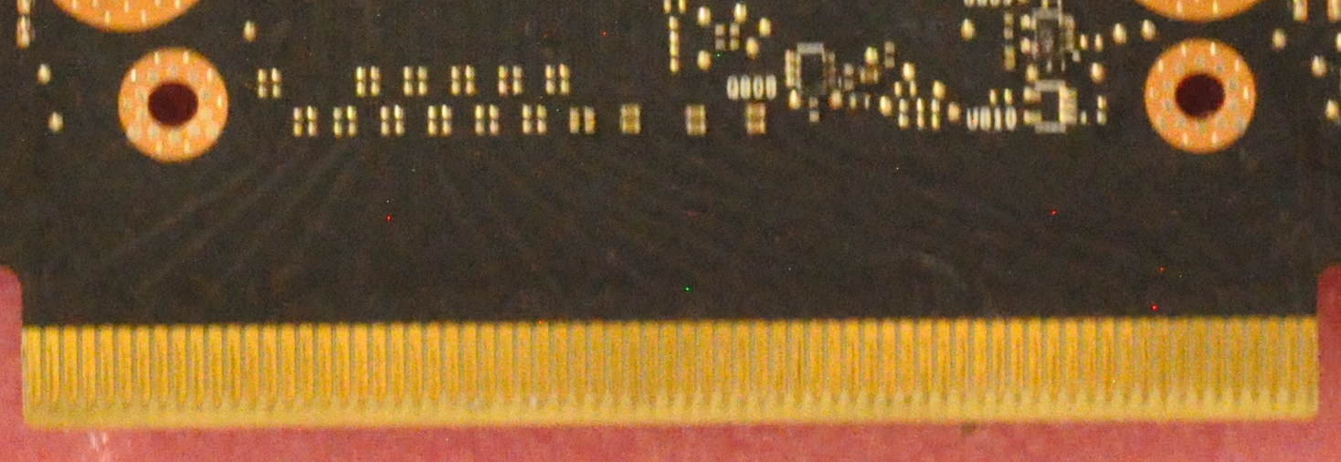
Finally, because the CMP 170HX uses the same Nvidia A100 circuit board, the gold fingers of the NV-Link interface exist, but the feature is unsupported with all components unpopulated on the PCB.
Discussion
Machine Balance and Arithmetic Intensity
As already mentioned, even though that the CMP 170HX has locked-down FP32 performance, there are still some floating-point workloads that can be accelerated by the CMP 170HX. In some cases, even up to the full HBM2e memory speed and beat the top-level customer-grade GPU: the RTX 4090. In the most extreme case (as in my FDTD demo), this can be done without bypassing the FMA throttling. One can often find them in memory-bound physics simulations. To understand why, one needs to make use of the concepts of machine balance, arithmetic intensity and roofline analysis.
Machine balance describes the balance between a processor’s memory and floating-point throughput. In the ideal world, this balance should be 1:1 so a processor can read or write memory as fast as it can perform an arithmetic operation. However, processors were and are improving at a faster rate than DRAM bandwidth for multiple reasons, such as the time it takes for the sense amplifier to read bits from capacitors, the impracticality of integrating large DRAM and CPU on the same silicon, or the resulting interconnect bottleneck between a processor and DRAM as off-chip data transfer is always slower than on-chip access.
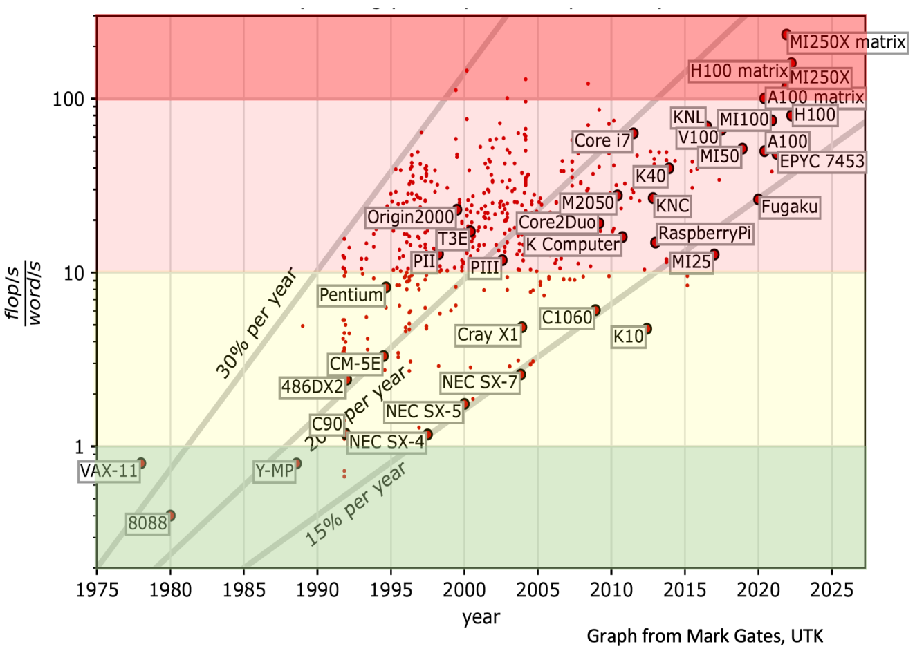
Hence, modern CPUs and GPUs tend to have a machine balance of 100:1 (for FP64). That is, one can only achieve the peak FLOPS of the processor if 100 floating-point operations are done for each integer read from memory - in other words (no pun intended), a compute kernel should have a high Arithmetic Intensity. Arithmetic Intensity is the balance between a program’s memory access operations and floating-point operations. For example, if a program needs to read 4 FP32s to calculate their average (using 3 adds and 1 multiplication), its arithmetic intensity is 0.25 FLOPs/bytes. That is, arithmetic intensity can be understood as a software balance in analogous to the machine balance.
In practical programs, the programmer will attempt to do as many useful computations as possible after memory is read using many tricks. But ultimately, the achievable intensity depends on the algorithm itself. For example, a good matrix multiplication program (the archetypal test is the LINPACK benchmark) is entirely compute-bound, as there are a whole lot of multiplications to do just after reading a single submatrix. Memory bandwidth does not matter in this application.
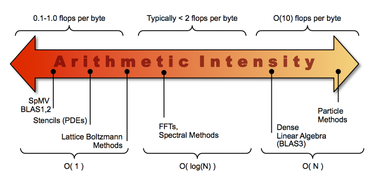
On the other hand, many types of scientific and engineering simulations are memory bandwidth bound. All they do is reading the simulation box from memory, moving it forward by 1 timestep, and writing it back to memory (think of a 2D or 3D convolution function in which the value of a single cell depends on the values of their surrounding cells, or think of a naive implementation of Conway’s Game of Life - real physics simulations of partial differential equations often work like that). The arithmetic intensity is often under 1.0 and performs poorly on modern hardware. The usable performance is 1% to 10% of the peak performance due to bandwidth limitation, which is far from what the processor core itself can do.
This is the notorious memory wall problem, to be accurate, the memory bandwidth wall problem (which is different from the memory latency wall problem).
Roofline Model
Since memory-bound number-crunching code is so prevalent in the scientific computing (or High-Performace Computing) world, practitioners established a simple graphical method named the roofline model as a quick guideline on program optimization, using only the ratio between floating-point operations and memory accesses.
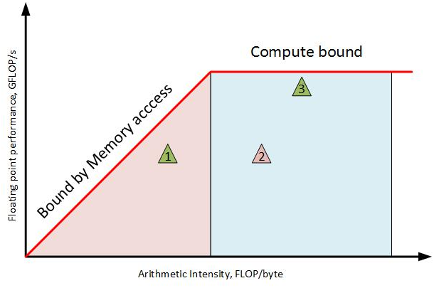
A naive roofline model is easy to graph. First, divide a processor’s peak floating-point throughput by its peak memory bandwidth. This gives the critical arithmetic intensity at which a memory-bound algorithm becomes a compute-bound one, known as the ridge point. Then, plot two segments, one from the ridge point to the origin at the left, another is a constant function equal to the machine’s peak floating-point performance, from the ridge point to the right. Then rescale the chart on a log-log scale.
Next, calculate the number of floating-point operations and the arithmetic intensity of your application and mark it on the plot. Many number-crunching kernels are simple, one can often look at the inner loop and count them by hand, only the source code and its runtime are needed as a result. To automate this process, one can use CPU performance counters and static analysis as well.
In the case of my CMP 170HX, I found my FDTD kernel performs 18 floating-point operations per cell, with an arithmetic intensity of 0.25 FLOPs/byte. At 10110 million cell updates per second, the achieved performance is 181.98 GFLOPS. For FluidX3D, 1 cell update takes 363 arithmetic operations consisting of 261 FP32 flops + 102 INT32 ops with 153 bytes of memory traffic. If one ignores INT32 bottleneck (it’s much faster than FP32 on the CMP 170HX), the arithmetic intensity would be 1.7 FLOPs/byte, and the achieved performance at 7684 cell updates per second is 1979.685 GFLOPS. Finally, I can create the following roofline model of this GPU with applications to two kernels: FDTD and FluidX3D (FP32/FP32, no FMA).

As one can see, even when the computing power is limited to 6 TFLOPS similar to a low-end desktop GPU, but both applications can greatly benefit from the 1350 GB/s memory bandwidth. For naive FDTD, due to its extremely low arithmetic intensity, it cannot even saturate the 394 GFLOPS FMA performance, explaining why it’s unaffected by Nvidia’s throttling.
Conclusion
Nvidia knows the hardware specs of the GA100 silicon are attractive to all HPC and AI users beyond mining, so they tried as best as they could to make this GPU totally useless for those purposes from different angles.
First and foremost, the FP32 FMA throughput restrictions makes the GPU almost useless for running ready-made software. As demonstrated here, this performance limit can sometimes be worked around by disabling FMA, making it acceptable for many memory-bound simulations. Unfortunately, due to the existence of other limitations, such as its low 8 GiB memory size, PCIe 1.0 x4 I/O bandwidth, the lack of NV-Link, and the lack of FP64 capability, these measures guaranteed the uselessness of the GPU in the vast majority of applications.
Overall, this GPU is mostly useless. It can still be useful only when your have a specific niche in which…
- Small-to-medium size runs that fits in 8 GiB.
- Mostly in-situ computation without doing any PCIe or NVLink transfers.
- You have a floating-point algorithm but extremely memory-bound that FLOPS is
completely irrelevant.
- Without disabling FMA, with an Arithmetic Intensity (AI) under 0.3 (FP32).
- After disabling FMA, with an Arithmetic Intensity under 4.6, but potentially requires modifications to standard and 3rd-party libraries.
- Or you have a memory-bound, all-integer workload (e.g. mining)…
Only then, it would be sensible to purchase this GPU.
I purchased this GPU specifically for running FDTD electromagnetic field simulations, the AI of its naive implementation is 0.25 FLOPs/bytes, so it still gives me a huge acceleration on par with the actual A100 and currently unmatched by everything else (if rumors are to be believed, RTX 5090 is eventually going to match it at 1.5 TB/s in 2024). Not the worst $500 I’ve spent.
It doesn’t change the fact that It’s still a case of caveat emptor, do not buy unless you know exactly what you’re buying.
VBIOS modding?
A natural question is whether the hardware performance limitation is implemented via fuses, or implemented via VBIOS firmware, and whether modifying the VBIOS can bypass these limits.
Unfortunately, all Nvidia GPUs since recent years have VBIOS digital signature checks, making VBIOS modification impossible. A few months ago, a bypass was found for RTX 20-series “Turing” based GPUs, unfortunately, it does not apply to Ampere GPUs. Currently, VBIOS modding is impossible for the foreseeable future.
Radeon VII - the alternative from AMD
The mining-special GPU market was not monopolized by Nvidia, there was strong competition from AMD as well - the mining-special Radeon VII (one can call them mining-special Instinct MI50).
Long story short, during the height of Ethereum mining, many board makers in China unofficially created a special version of the Radeon VII by omitting components of the Instinct MI50 circuit board - the resulted GPU is a weird hybrid between Radeon VII and the Instinct MI50 - it has the Instinct MI50 circuit board with the Instinct MI50 passive cooler suitable for datacenter usage, on the other hand, the circuit configuration is actually a desktop Radeon VII, but it cannot be called a desktop card either as the video output is often omitted. Regardless, since the Radeon VII is more or less a remarketed accelerator GPU for gaming and uses basically the same Instinct MI50 silicon, both cards are practically the same thing, and it doesn’t matter which one is which.
In China, these GPUs are currently sold at ~$100. More amazingly, they are pre-modded with the Radeon Pro VII VBIOS with 11 TFLOPS of FP32 and unlocked 5.5 TFLOPS FP64 - just like the real MI50, making them possibly the accelerators with the highest price-performance ratio of all time. The only criticism I have is Radeon VII’s relatively inefficient memory controller, that often causes considerable under-utilization of its 1 TB/s HBM2 bandwidth.
Still, if you want to buy a mining-special GPU for cheap to run compute workloads, I personally highly recommend this mining-special Instinct MI50 (Radeon VII) over the Nvidia CMP 170HX if your application is not CUDA-specific.
I plan to review this GPU soon. Because of the lack of restrictions, I’m not going to analyze the GPU in depth as it behaves as a standard GPU as one normally expects, the focus of that article is going to be a watercooling mod tutorial for homelab use… There is a lot that can be said for its bandwidth efficiency problem, which seems to be an architectural problem across Vega GPUs and is currently poorly understood due to the lack of documentation - but I’m not sure if I have the patience to cover those topics.
Appendix 0: Disabling FMA Usage by Source Code or Runtime Modification
OpenCL
Source Code Modification
An FMA or MAD instruction - which are all throttled on the CMP 170HX - may be generated by the OpenCL compiler under the following two conditions:
-
The source code explicitly uses the OpenCL functions
fma()ormad(). -
The compiler implicitly transforms the expression
a * b + ctofma(a, b, c)ormad(a, b, c)through a process called FP contraction. This may occur even without enabling fast math or unsafe math optimizations - which merely increases the complier’s aggressiveness of doing so.
Thus, to prevent the OpenCL compiler from using MAD and FMA instructions,
two things need to be done - first, remove all usages of fma() and mad(),
and also to turn FP contraction off. An easy workaround is to
include the following code in front of all OpenCL source files:
/* shadows the OpenCL builtin fma() and mad() functions */
#define fma(a, b, c) ((a) * (b) + (c))
#define mad(a, b, c) ((a) * (b) + (c))

/* disable FP contraction */
#pragma OPENCL FP_CONTRACT OFF
FluidX3D
When testing FluidX3D, a similar two-line patch was used, which is reproduced below:
diff --git a/src/lbm.cpp b/src/lbm.cpp
index d99202f..28aeb25 100644
--- a/src/lbm.cpp
+++ b/src/lbm.cpp
@@ -286,6 +286,8 @@ void LBM_Domain::enqueue_unvoxelize_mesh_on_device(const Mesh* mesh, const uchar
 }

 string LBM_Domain::device_defines() const { return
+       "\n     #pragma OPENCL FP_CONTRACT OFF"  // prevents implicit FMA optimizations
+       "\n     #define fma(a, b, c) ((a) * (b) + (c))"  // shadows OpenCL explicit function fma()
        "\n     #define def_Nx "+to_string(Nx)+"u"
        "\n     #define def_Ny "+to_string(Ny)+"u"
        "\n     #define def_Nz "+to_string(Nz)+"u"
PoCL
The Nvidia OpenCL compiler is proprietary inside libnvidia-opencl.so, unlike
AMD GPUs for which its driver simply invokes clang. Thus, there’s no transparent
way to disable FMA and MAD globally at the compiler level (apart from reverse
engineering and modifying the Nvidia binaries). Each OpenCL program has to
be painstakingly modified individually.
A potential workaround is intercepting the call into clBuildProgram() to
modify the compiler options. Unfortunately, the OpenCL specification provides
no compile-time options to disable floating-point contraction in the form of
a command-line off/on switch. Yet another workaround can be intercepting
clCreateProgramWithSource() to insert the aforementioned code on the fly. But
this is a rather tedious and is left as an execrise for the reader.
Another possible and more straightforward hack is to replace the Nvidia OpenCL
runtime altogether with PoCL - a free and portable OpenCL runtime based on
LLVM/clang with the ability to target Nvidia PTX. By modifying the PoCL function
pocl_llvm_build_program(), the clang flag -ffp-contract=off is passed
unconditionally to disable FP contraction. In addition, PoCl’s OpenCL standard
library functions fma() and mad() also need to be redefined as plain
a * b + c without FP contraction. This is implemented by the following patch,
allowing one to run pre-existing OpenCL programs without any source code
modification.
diff -upr pocl-4.0/lib/kernel/fma.cl pocl-4.0/lib/kernel/fma.cl
--- pocl-4.0/lib/kernel/fma.cl	2023-06-21 13:02:44.000000000 +0000
+++ pocl-4.0/lib/kernel/fma.cl	2023-10-28 12:44:58.283185457 +0000
@@ -24,4 +24,5 @@

 #include "templates.h"

-DEFINE_BUILTIN_V_VVV(fma)
+#pragma OPENCL FP_CONTRACT OFF
+DEFINE_EXPR_V_VVV(fma, a*b+c)
diff -upr pocl-4.0/lib/kernel/mad.cl pocl-4.0/lib/kernel/mad.cl
--- pocl-4.0/lib/kernel/mad.cl	2023-06-21 13:02:44.000000000 +0000
+++ pocl-4.0/lib/kernel/mad.cl	2023-10-28 12:45:02.093091566 +0000
@@ -24,4 +24,5 @@

 #include "templates.h"

+#pragma OPENCL FP_CONTRACT OFF
 DEFINE_EXPR_V_VVV(mad, a*b+c)
diff -upr pocl-4.0/lib/CL/pocl_llvm_build.cc pocl-4.0/lib/CL/pocl_llvm_build.cc
--- pocl-4.0/lib/CL/pocl_llvm_build.cc	2023-06-21 13:02:44.000000000 +0000
+++ pocl-4.0/lib/CL/pocl_llvm_build.cc	2023-10-28 11:36:33.961059705 +0000
@@ -333,10 +333,8 @@ int pocl_llvm_build_program(cl_program p
   if (fastmath_flag != std::string::npos) {
 #ifdef ENABLE_CONFORMANCE
     user_options.replace(fastmath_flag, 21,
-                         "-cl-finite-math-only -cl-unsafe-math-optimizations");
+                         " ");
 #endif
-    ss << "-D__FAST_RELAXED_MATH__=1 ";
-    fp_contract = "fast";
   }

   size_t unsafemath_flag = user_options.find("-cl-unsafe-math-optimizations");
@@ -346,11 +344,14 @@ int pocl_llvm_build_program(cl_program p
     // this should be almost the same but disables -freciprocal-math.
     // required for conformance_math_divide test to pass with OpenCL 3.0
     user_options.replace(unsafemath_flag, 29,
-                         "-cl-no-signed-zeros -cl-mad-enable -ffp-contract=fast");
+                         " ");
 #endif
-    fp_contract = "fast";
   }

+  // HACK: disable FP contraction unconditionally
+  fp_contract = "off";
+  ss << " -ffp-contract=off ";
+
   ss << user_options << " ";

   if (device->endian_little)
It’s worth noting that the patch is incomplete, as OpenCL has more fma() and mad()
variants than what are patched here, such as mad24(), mad_hi(), and mad_sat().
CUDA
To disable FP contraction, pass the option -fmad=false to nvcc.
Again, like OpenCL, it’s also possible to use FMA and MAD via multiple
built-in functions. Since nvcc is proprietary, again, there’s no
transparent way to disable FMA and MAD globally at the compiler level -
apart from reverse engineering and modifying the Nvidia binaries, or
implementing a preprocessor or debugger-like interceptor to modify
the source on-the-fly.
On the other hand, just like OpenCL, it’s possible to compile CUDA via LLVM/clang and target Nvidia PTX. Thus, in principle, it should be possible to create a patched LLVM/clang for this purpose in analogous to PoCL.
SYCL
Currently there are two full-feature SYCL implementations - an LLVM
fork named Intel DPC++ and an LLVM plugin named AdaptiveCpp (previously
known as OpenSYCL and hipSYCL). One can use the standard clang
command-line option -ffp-contract=off. Like CUDA, the problem of
built-in functions remain.
Limitations
Although this section demonstrated some possible ways to modify the program source code or GPGPU runtime to avoid FMA and MAD usages, in practice, it can be difficult if not impossible to completely avoid FMA.
As I already showed, a transparent compiler/runtime patch is not as easy as toggling a option, as it doesn’t affect the behavior of built-in functions. An invasive patch to the compiler may be needed to completely remove FMA/MAD code generation.
Furthermore, even if one can patch the affected applications and runtimes, the problem of binary programs and standard libraries remain. Sometimes, GPU kernels are precompiled and shipped in machine code or assembly form, this is the case for proprietary software, and sometimes also the case for standard libraries. In fact, most HPC libraries contain hand-tuned assembly routines that heavily rely on FMA. Thus, the modification required to remove FMA/MAD usages from a codebase is likely very complicated unless the codebase is self-contained.
Not to mention that removing FMA changes the rounding behavior from 1 rounding to 2 roundings, thus pontentially compromising the numerical integrity of a simulation and making it untrustworthy if the code was written in a way that requires FMA to preserve precision.
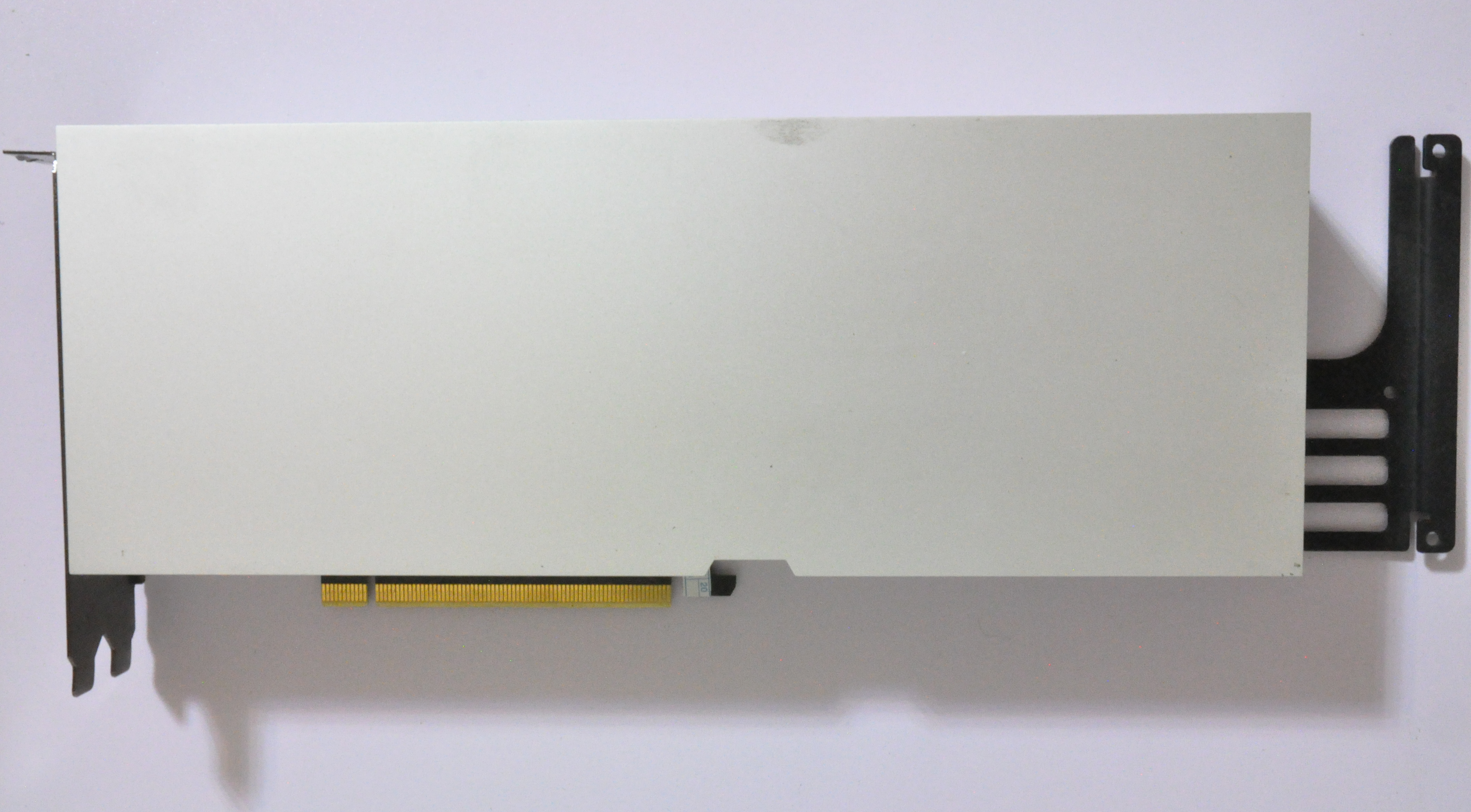
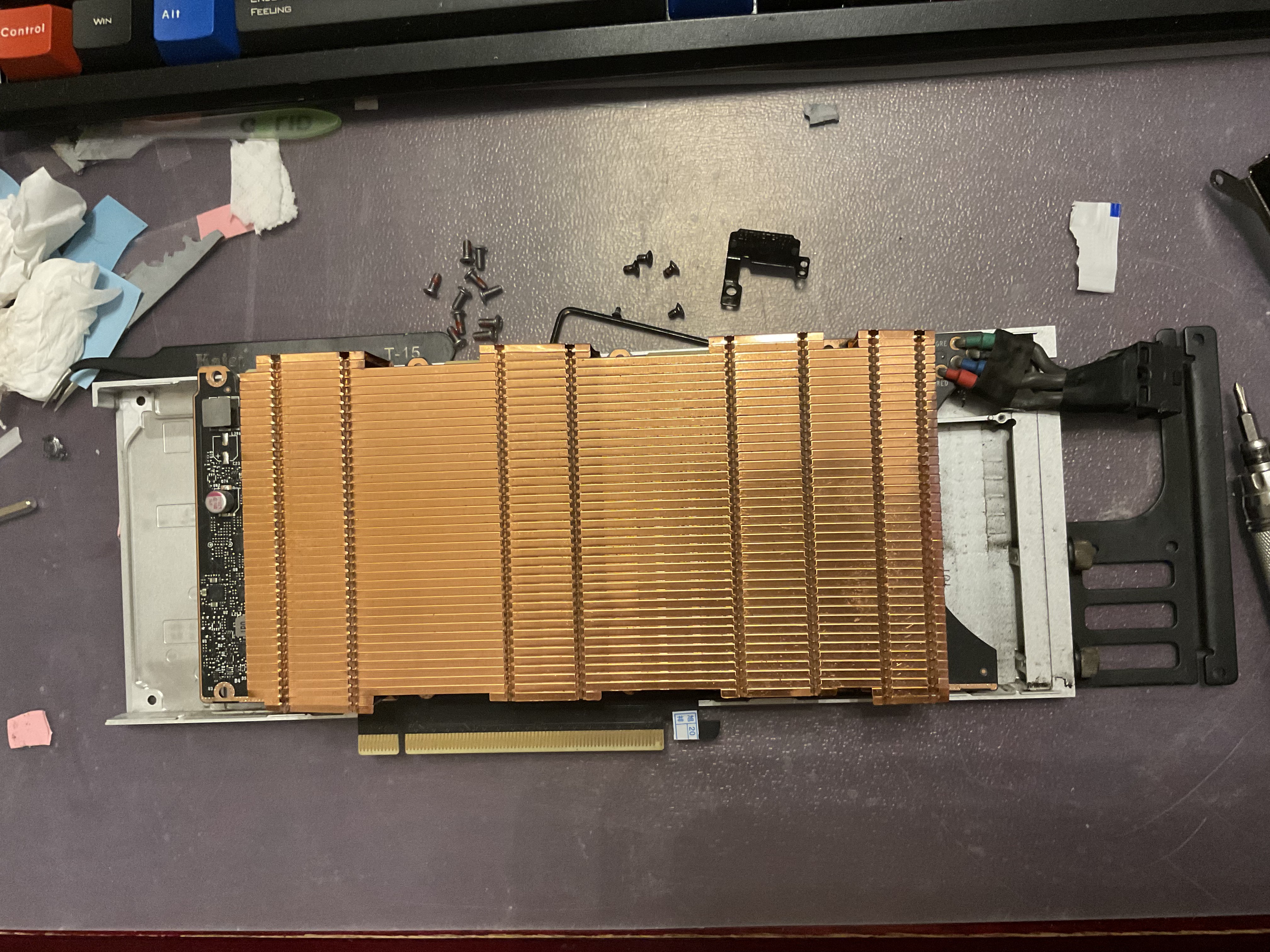
Appendix 1: Teardown
Circuit Board Separation
The following procedures separate the circuit board from its chassis and cooler.
Videos
Step 6, Step 7 and Step 9 can be tricky. Consider the fact that Step 7 initially confused even LinusTechTips, refer to following two YouTube videos (in Chinese) for visual demonstrations of the removal process.
Understanding the language is optional, but the second video has YouTube captioning and can be auto-translated to English. It’s posted by 技数犬, which is a Taobao vendor of aftermarket mod kits for many compute cards to allow the use of off-the-shelf AIO watercoolers (not used in my watercooling setup).
Procedures
It boils down to the following steps:
-
Remove 4 screws on the PCIe mounting bracket on the left. Save the PCIe bracket for later use.
-
It’s not necessary to remove the mounting bracket on the right (the opposite side of the PCIe slot bracket). Do not waste time on it.
-
Flip the card, remove 10 screws on the back side of the card.
-
Flip the card again, now open the front cover of the cooler, the PCIe bracket should also come off, revealing a massive heatsink.
-
Unscrew and remove the bracket on top of the power cable on the top right, which is holding the power cable and the connector in place.
-
Free the power cable away from the backplane by prying it away. The cable is squeezed into the backplane, and can be difficult to remove. Use a plastic spudger to pry it away from the board. Unless the power cable / connector is freed, the circuit board cannot move freely.
- Use videos for guidance.
-
Pay attention to the fact that the entire circuit board is inserted into the bottom backplane by sliding the PCIe connector into an open slot on the backplane, thus, the circuit board cannot be lifted off vertically as it’s embedded into the backplane.
-
To remove the circuit board (and the bolted-on heatsink), move the circuit board upward horizontally (to the opposite direction of the PCIe connector). After the PCIe connector moves a bit away from the slot on the backplane, lift the circuit board vertically while keep moving it upward horizontally. The circuit board is now separated from the backplane (as shown in the photo below).
-
Use videos for guidance.
-
- Remove 4 spring-loaded screws on the backside of the PCB, keep the 4 washers for later use, remove the mounting bracket.
-
There’s no more screws holding the heatsink, and it can be directly removed. However, the thermal paste often works like an adhesive. In this case, pry the cooler away from the circuit using a plastic spudger from the top side of the cooler at where there’s no components on the circuit board. Put the card on a flat desk, rotate the card by 180 degrees, and insert the plastic spudger onto the bottom (top before the rotation) side of the card, and pry it upward while holding the heatsink (to prevent the heatsink from smashing the circuit board).
-
Cooler and circuit board are separated.
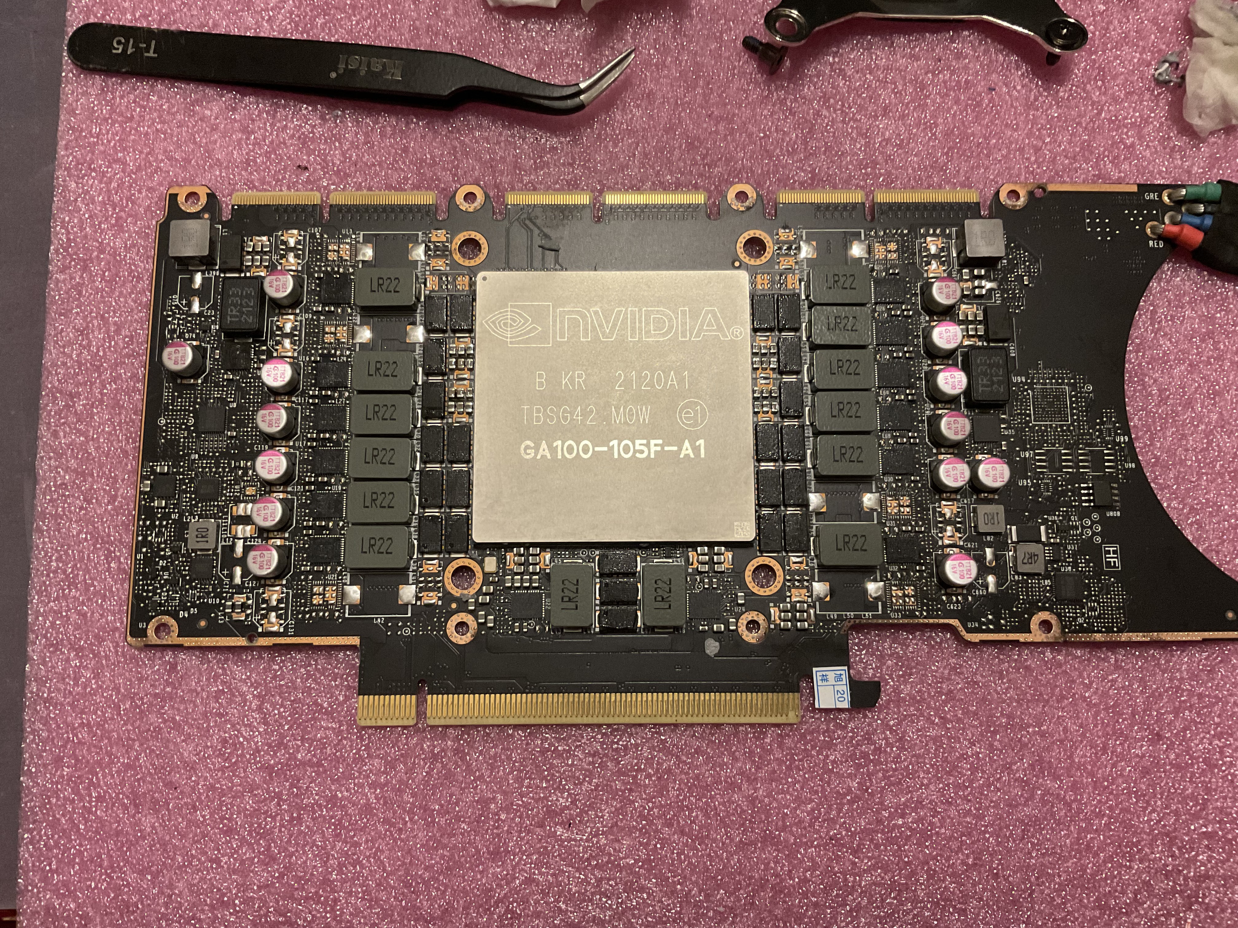
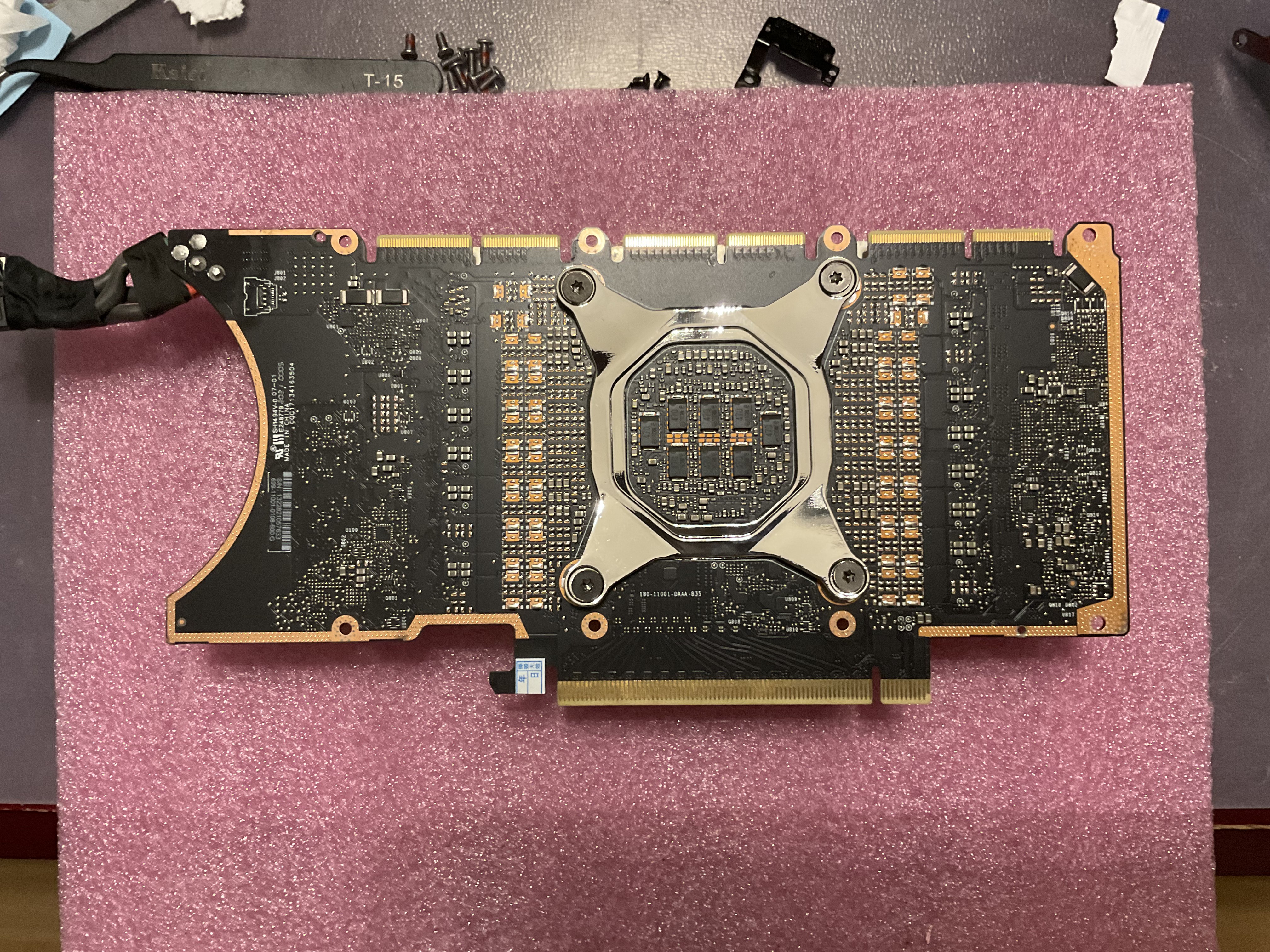
Circuit Board
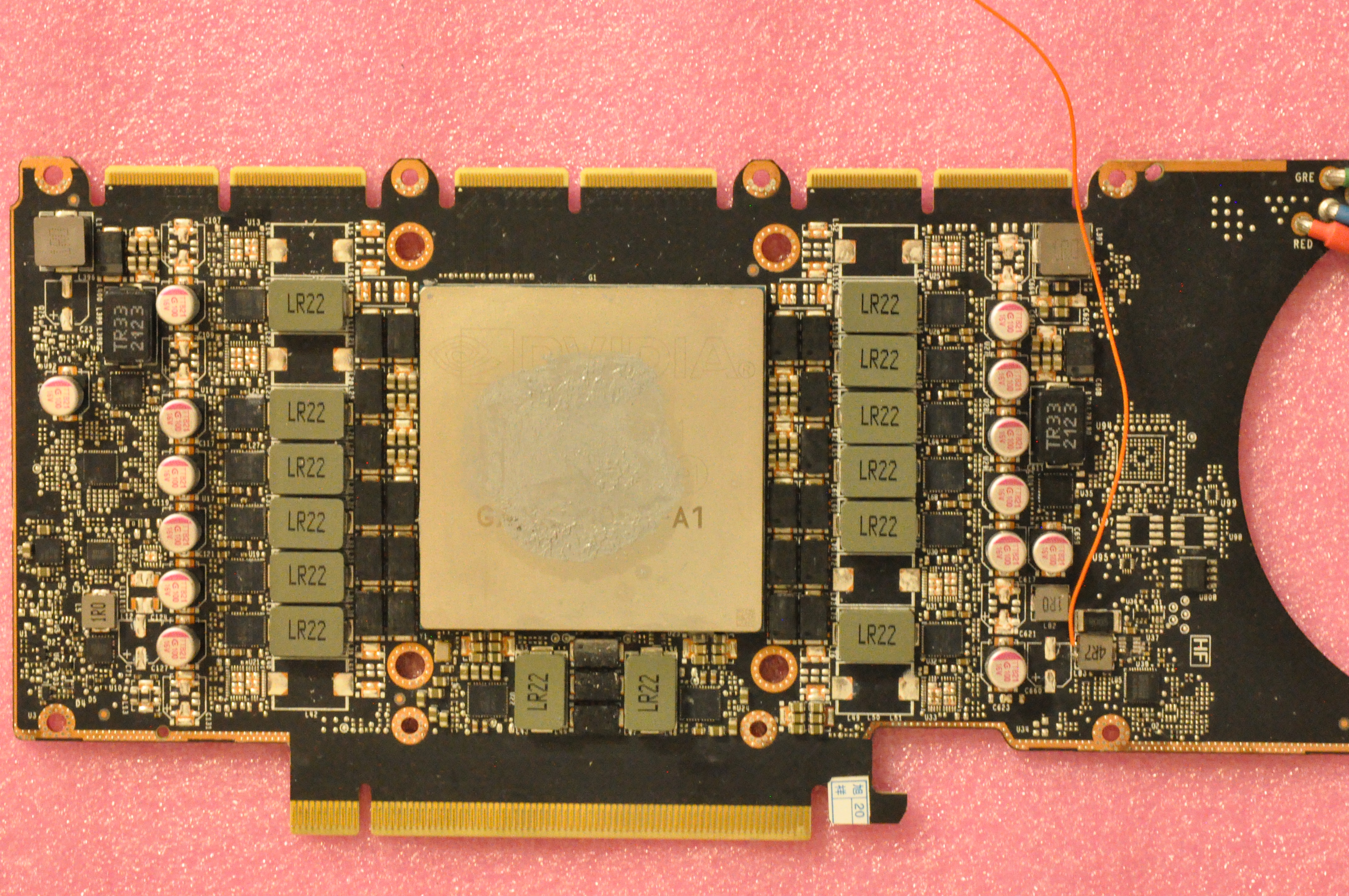
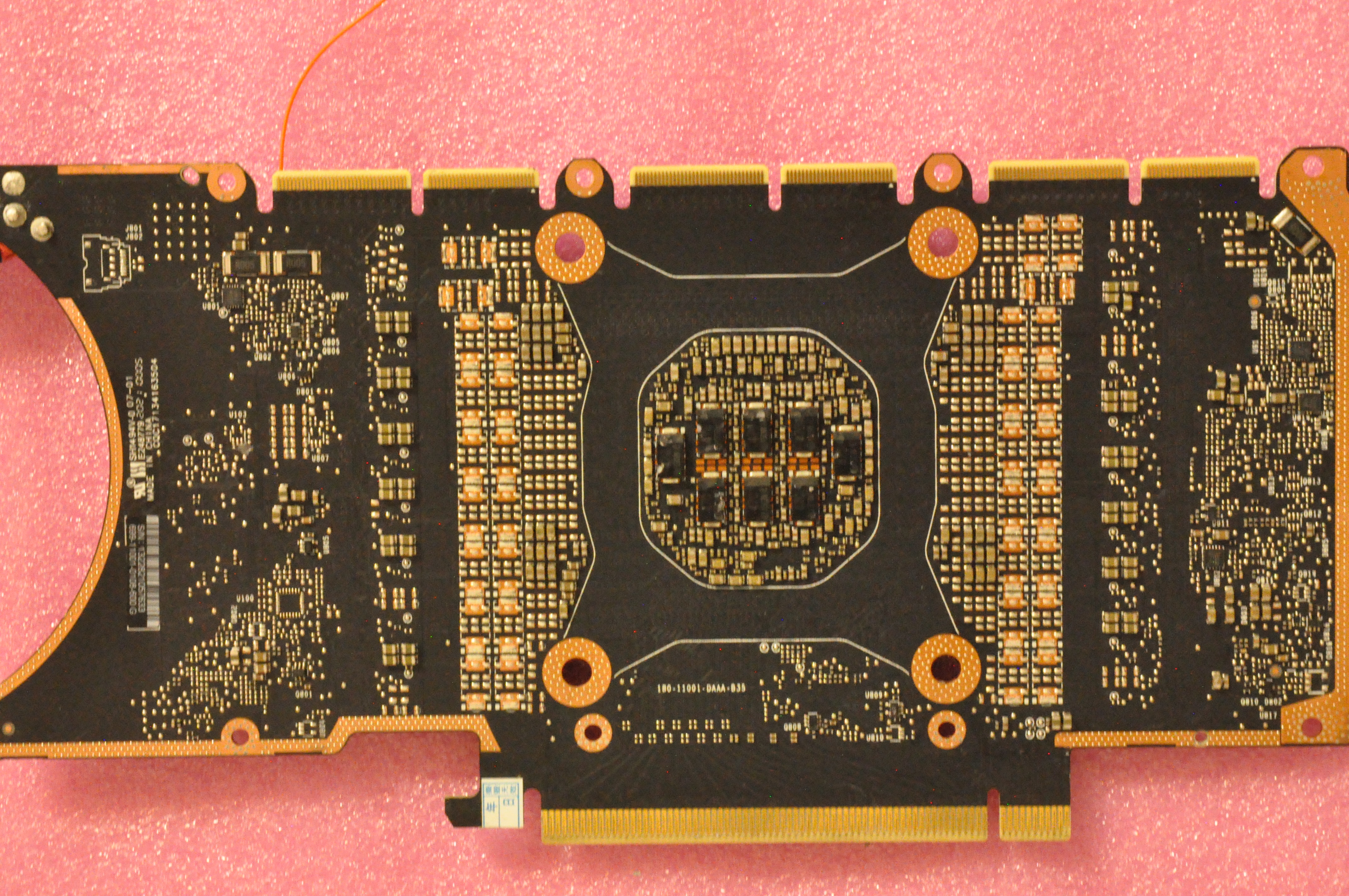
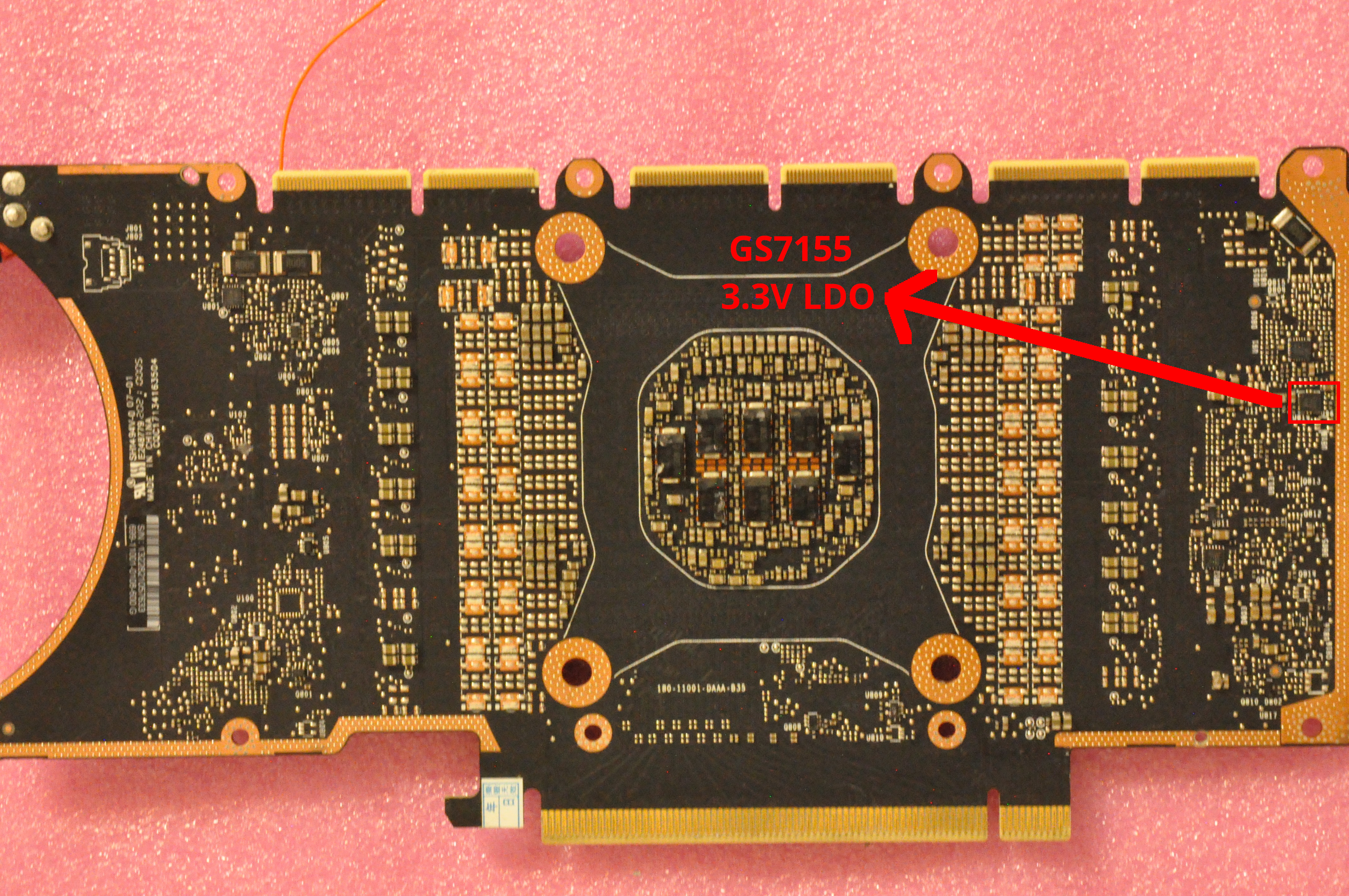
The Nvidia CMP 170HX uses a circuit board nearly - if not completely - identical
to the Nvidia A100 (40 GiB). The only difference is the model number of the
GPU ASIC GA100-105F-A1 which seems to be a cut-down version of the full
GA100. The circuit board also has many unpopulated components, including
omitted VRM phases by unpopulating DrMOS transistors and their output
inductors, ICs related to the NV-Link interface are also missing.
Otherwise, even the component reference designators on the circuit board perfectly match the leaked electrical schematics of the Nvidia Tesla A100 reference design (found online) - yes, the A100 was still internally named Tesla when the GPU was being designed.
All hardware modifications to the Nvidia A100 (40 GiB, not 80 GiB), such as watercooling solutions like waterblocks and modification kits, are equally applicable to the CMP 170HX. Thus, for those who’re playing along at home, if anyone wants perform a risky modification to their expensive Nvidia A100 for workstation use, it might be a good idea to practice this modification on an inexpensive CMP 170HX first.
Appendix 2: Watercooling
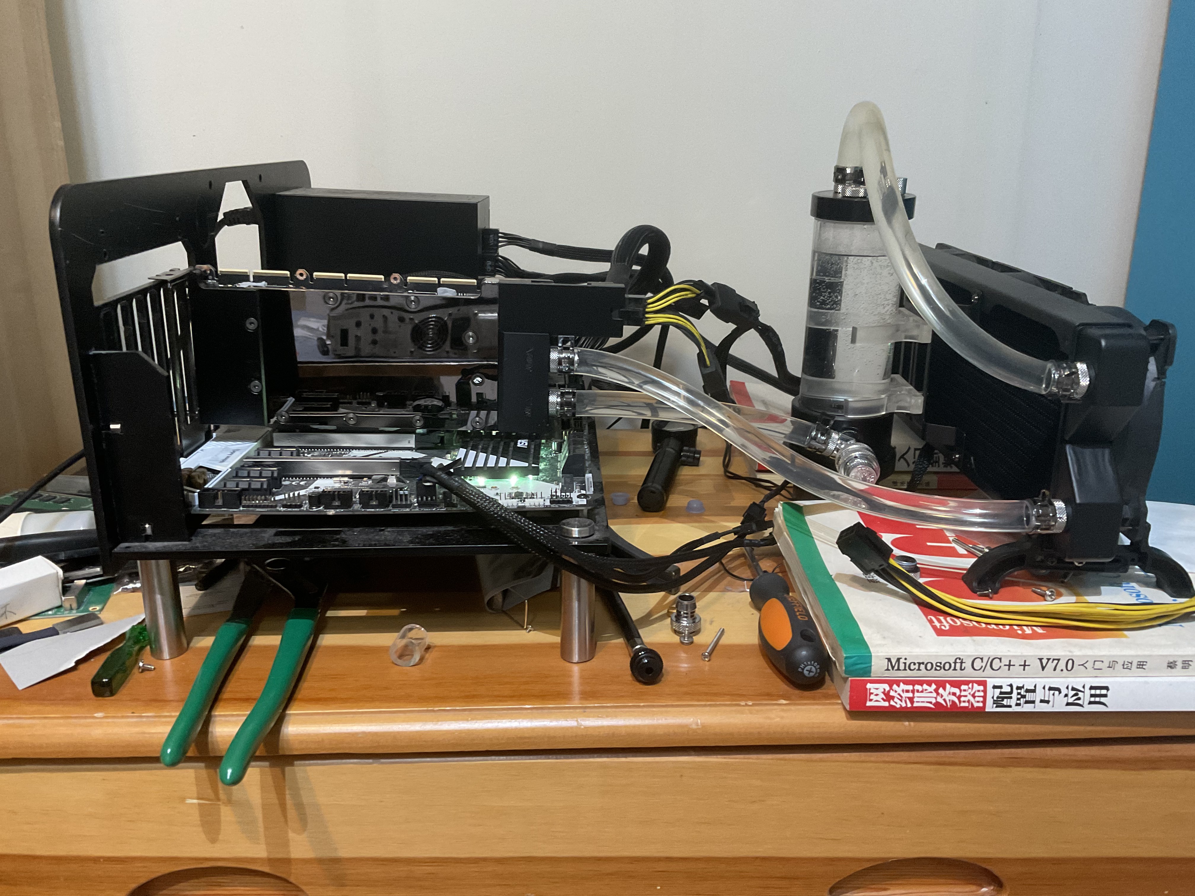
When attempting to use server GPUs for home/office workstation applications, cooling is a standard problem. Most server-grade GPUs use passive coolers and they’re designed to be cooled by high-RPM fans on a server chassis. Even if fans can be installed in the original way or via a custom mod, these passive coolers often need a strong airflow to work properly, creating a noise level unacceptable outside a data center.
Fortunately, for popular compute-only GPUs, ready-made waterblocks often exist, making watercooling a common solution using off-the-shelf parts. Watercooling has its downsides, but as long as precautions are carefully followed - which shouldn’t be difficult for the experienced home lab experimenters who regularly purchased used hardware - watercooling provides cool temperature and quiet operation in exchange. This is quite important when you’re running number-crunching simulations while sleeping next to it…
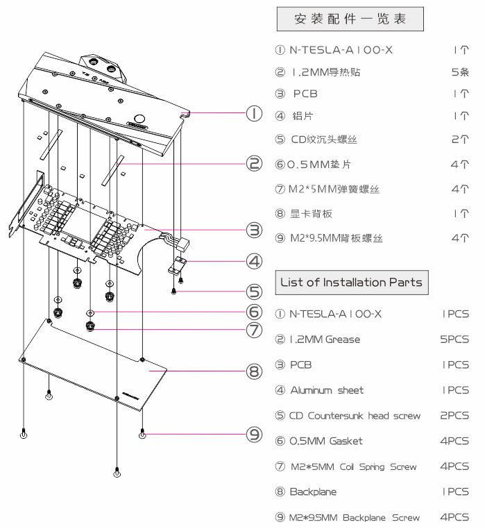
To cool my Nvidia CMP 170HX, I found the Bykski N-TESLA-A100-X-V2 waterblock,
which is compatible with Nvidia A100 40 GB, Nvidia CMP 170HX, and the
Nvidia A30 24 GB circuit boards. In China, it’s currently sold at a
price of 680 CNY (~100 USD). The bykski.us distributor site is selling
it for $300, I suggest ordering it from AliExpress for less than $150.
The waterblock accepts standard G1/4 fittings and can be included in
any water loop. If this is your first installation, you can find more
information on connecting a pump, radiator or reservoir into the water
loop (none is included) on most PC enthusiast websites.
Make sure you do not confuse the Nvidia Tesla 40 GB version with the 80 GB
version, which are incompatible. There is also an earlier version of the
same waterblock without V2 in its model number, V2 uses all-metal
construction while the non-V2 uses transparent acrylic. Since the metal
revision was made for a reason (enhanced durability), it’s better to
avoid the non-V2 models.
Procedures
The Bykski waterblock has no user manual. The provided online user guide is more of a quick start guide than a user manual, with a two-sentence instruction.
Those who can, do.
Those who can’t, write.
Those who can’t write, sell waterblocks at Bykski.
I also found the included hex wrench was the wrong size (so be sure to order a set of metric hex wrenches if you don’t have one already). Otherwise, it performs great if you manage to correctly install it.
Which is a big if… My GPU stopped working soon after the waterblock installation (but I was able to fix that myself). I suspect it was either a pre-existing fault due to heavy mining by its previous owner, or was caused by my improper waterblock installation - if the latter was the case, the lack of a proper user manual from Bykski was certainly an important contributing factor - but fear not, this blog post already went ahead of you and ironed out a smooth path. You can refer to the following instructions to do the same watercooling mod, with the foresight of many pitfalls in order to avoid damaging your GPU.
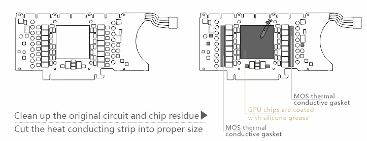
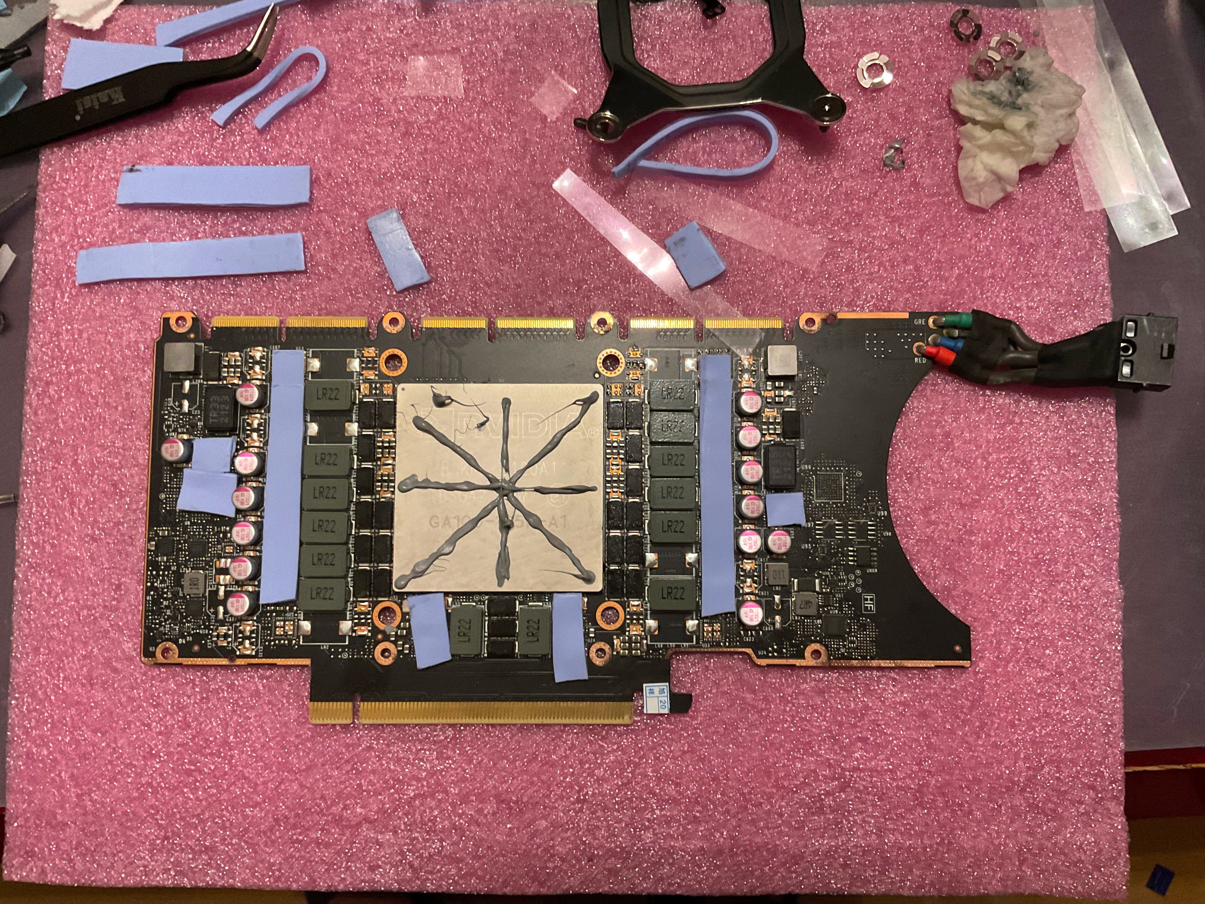
-
Cut and place included thermal pads on the MOSFETs (DrMOS) on the left and right sides of the GPU ASIC. Important: All unpopulated IC footprints must also be covered by thermal pads to prevent a short circuit. I suspect a short thermal pad cut missing the empty IC footprint on the topmost position was how I damaged my card.
-
Similarly, apply thermal pads on the bottom left and right side of the GPU ASIC.
-
Similarly, apply thermal pads to the PMIC on the right side of the GPU ASIC between an inductor and a capacitor.
-
Similarly, apply thermal pads to the two PMICs on the left side of the GPU ASIC below the 3.3 µH inductor.
-
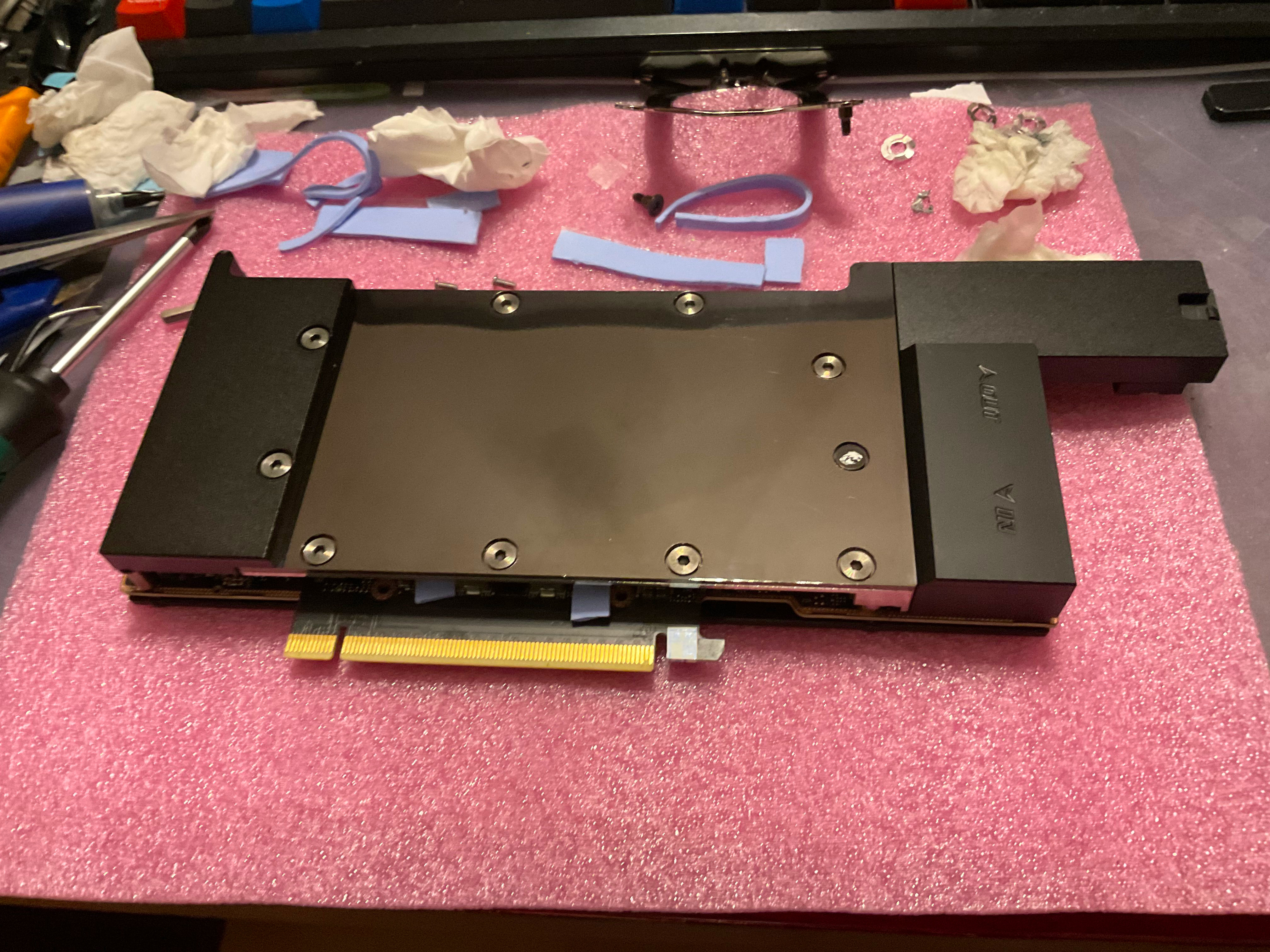
Apply thermal paste to the GPU ASIC. After completing these steps, the GPU should look similar to the following photo.
- Flip the waterblock, remove the power connector holder cover (labeled Item 4 in the exploded-view diagram below) by unscrewing the two hex nuts (labeled Item 5) with a hex wrench. The included hex wrench from the waterblock was the wrong size, use your own.
-
Place the waterblock onto the GPU. Important: Before placement, it’s good idea to visually double check whether the IC areas in contact of the pillars on the waterblocks are fully covered with thermal pads.
-
Flip the GPU, move the waterblock to align the four mounting screw holes of the waterblock with the PCB.
-
Find the 4 washers you’ve saved in the teardown step 8. For washers, use the original ones from the GPU, avoid the plastic washers from the waterblock. For spring-loaded screws, avoid the original screws and use the screws from the waterblock. Place one washer on one mounting hole, and install only one 1 spring-loaded screw, for now, do not install all 4 screws.
-
Insert the power connector by squeezing it into the slot on the waterblock on the top right corner (make sure the cover has already been removed in Step 6). The stiff power cable exerts force on the entire PCB, making it difficult to install if the waterblock is already fully screwed.
-
If there are still difficulties during installation, unscrew and lift the waterblock completely, insert the power connector in its position before placing the waterblock back. In this case, considerable force is needed to overcome the stifness of the power cable when aligning the circuit board with the waterblock. Screw the waterblock immediately after the first signs of an alignment using Step 9.
-
If the waterblock is lifted and remounted, be sure to double check that no thermal paste has shifted in position. The thermal pads can stick onto the waterblock and land on an unpredictable location later.
-
-
Adjust the waterblock for any misalignment, place the remaining 3 washers onto the mounting hole, and install 3 spring-loaded screws included with the waterblock. Important: After the waterblock is screwed in, now it’s a good time to peek into the circuit board to see whether the thermal pads are making good contact with the pillars to cool the MOSFETs. The thermal pads included with the waterblock should always work, but in case you’re using your own, now it’s time to spot any thickness issues.
-
Reinstall the power connector holder bracket back onto the waterblock with a hex wrench.
-
Grab the backplane (included with the waterblock) from its packaging. Using the backplane is optional, but it reduces the chance of damaging the back side of the PCB in case of mishandling.
-
Find the PCIe slot bracket you’ve saved during teardown in Step 1, align and place it on the left side of the circuit board. Important: Do not skip this step, the additional height of the PCIe slot bracket likely ensures a proper spacing between the backplane and the circuit board, thus preventing potential short circuits. I suspect this was how I damaged my card.
-
Align and place the included backplane on top of the circuit board (on the left, the PCIe bracket is sandwiched between the PCB and the backplane). On the left, the screw holes of the PCB, the PCIe bracket, and the backplane should be aligned. After successful alignment, immediately install two 9.5 mm M2 screws (included with the waterblock).
-
Install the remaining two 9.5 mm M2 screws to secure the backplane.
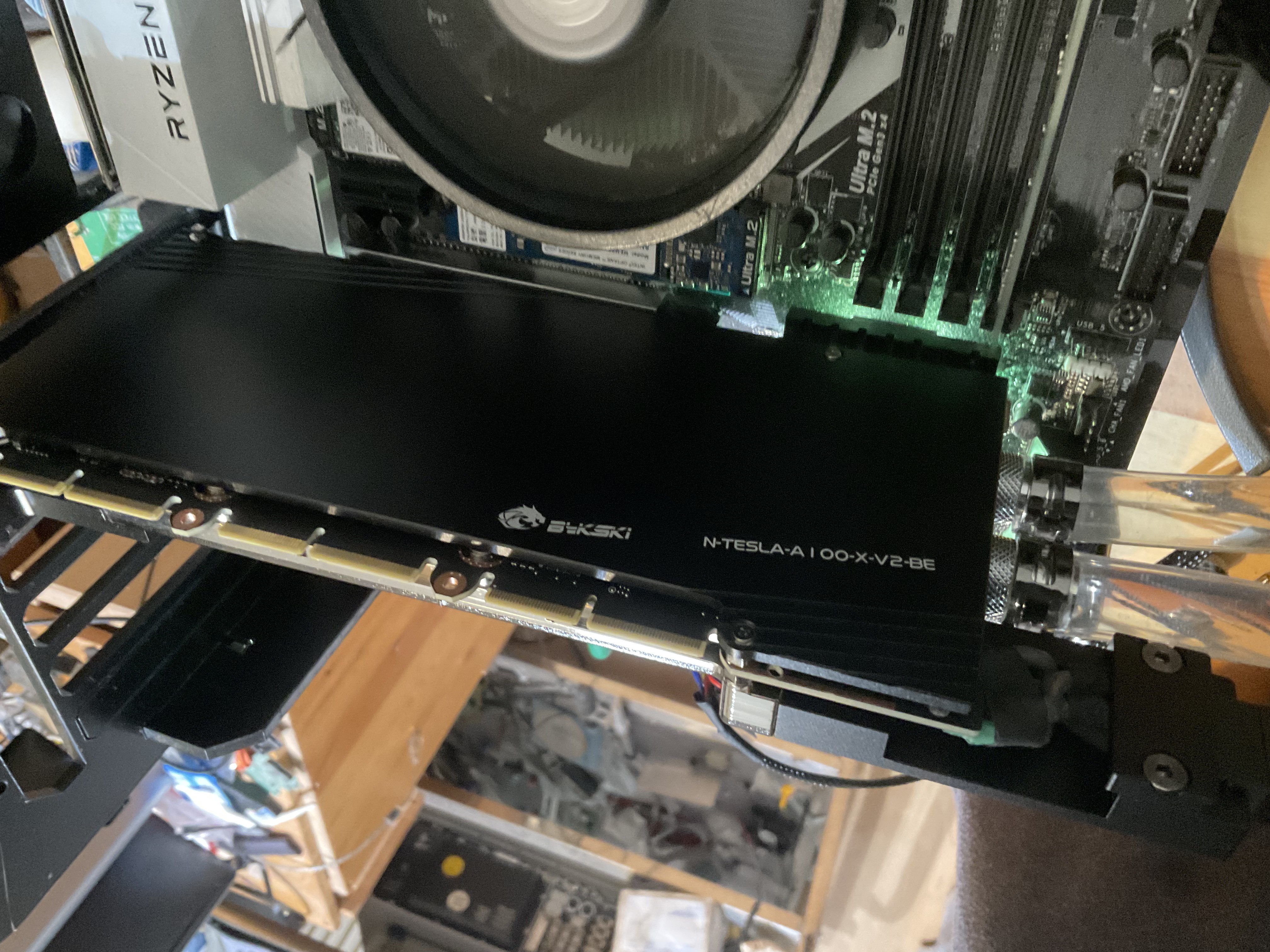
- Waterblock installation complete, connect the water block into your water loop. Use a leak tester to pressurize the water loop for 15 minutes to verify the loop’s air tightness before adding coolant.
Temperature
Using a 360 mm, 3-fan radiator, the GPU’s temperature when idle is 30 degrees C at 30 watts.
In a FluidX3D simulation using FP32/FP16S mode with FMA disabled, the power consumption is 180 watts. After running this stress test for half an hour, the GPU temperature reached 45 degrees C. Both the fan and pump speeds were kept at a minimum, allowing silent operation during GPU number-crunching. Even lower temperature may be possible at a higher fan speed.
When I was dry-running the card for an initial test without coolant (not recommended! Make sure to power the system off within 5 minutes), I also noticed a curious positive feedback loop between the GPU temperature and its power consumption, creating thermal runaway. Initially, the idle power consumption was around 40 watts, but it gradually rised to 60 watts at 80 degrees C and was still increasing before I powered it off - I later found many other PC reviewers reported similar findings. This was likely an effect caused by higher CMOS leakage current at higher temperatures, which in turn creating more leakage current and an even higher temperature… Hence, good cooling can often reduce an IC’s junction temperature by more than their cooling capability alone due to this second-order effect.
Appendix 3: Repair
My Nvidia CMP 170HX malfunctioned soon after I received it and performed the first attempt at watercooling modification. The GPU operated for an hour before it dropped off from the PCIe bus, and could no longer be detected after this incident.
Such is the well-known risk of purchasing or modding decommissioned hardware, or doing both at the same time! - never bet more than you can afford to lose.
It was either a pre-existing fault (perhaps the circuit was already marginal after heavy mining), or due to my improper watercooling installation - a few sentences in the installation procedures are marked as important in bold fonts for a reason… If it was indeed damaged from my improper installation, the lack of a proper user manual from Bykski was certainly an important contributing factor - but fear not, this blog post already went ahead of you, and ironed out a smooth path. You can refer to the previous instructions to see many pitfalls to avoid damaging your GPU.
I was able to repair the problem myself with the help of my electronics home lab (which is not a coincidence, since I bought this GPU specifically to write electromagnetic simulation code for circuit board designs…), and with the help of leaked Nvidia Tesla A100 schematics. Thanks to whoever who leaked them - My repair is otherwise impossible.
Reference designs and OEM circuit schematics are routinely leaked online or sold on the gray markets to repair technicians. This includes most desktop and laptop motherboards and GPUs. I’m just surprised that someone actually decided to leak the $10,000 server-grade A100 together with other conventional RTX 3080 and 3090 desktop GPUs.
As I had no prior experiencing on troubleshooting video cards, I also used the help of Nvidia Pascal GPU Diagnosing Guide on repair.wiki and also a few repair videos to learn what to expect - including the trick of using output inductors as test points of DC/DC converters - on my own circuit boards, I always used the output capacitors or dedicated test points and never realized this shortcut…
The GPU repair song
To The Army Goes Rolling Along:
Short the rail, fry the core,
Roll the coils across the floor,
And the system is going to crash.
MCUs smashed to bits
Give the scopes some nasty hits
And the system is going to crash.
And we’ve also found
When you turn the power up
You turn VRMs into trash.Oh, it’s so much fun,
Now the GPU won’t run
And the system is going to crash.Shut it down, pull the plug
Give the core an extra tug
And the system is going to crash.
Mem’ry chips, one and all,
Toss out halfway down the hall
And the system is going to crash.
Just flip one switch
The PWM will cease to twitch
MOSFETs will crumble in a flash.
When the GPU
Only renders magic smoke
Then the system is going to crash.
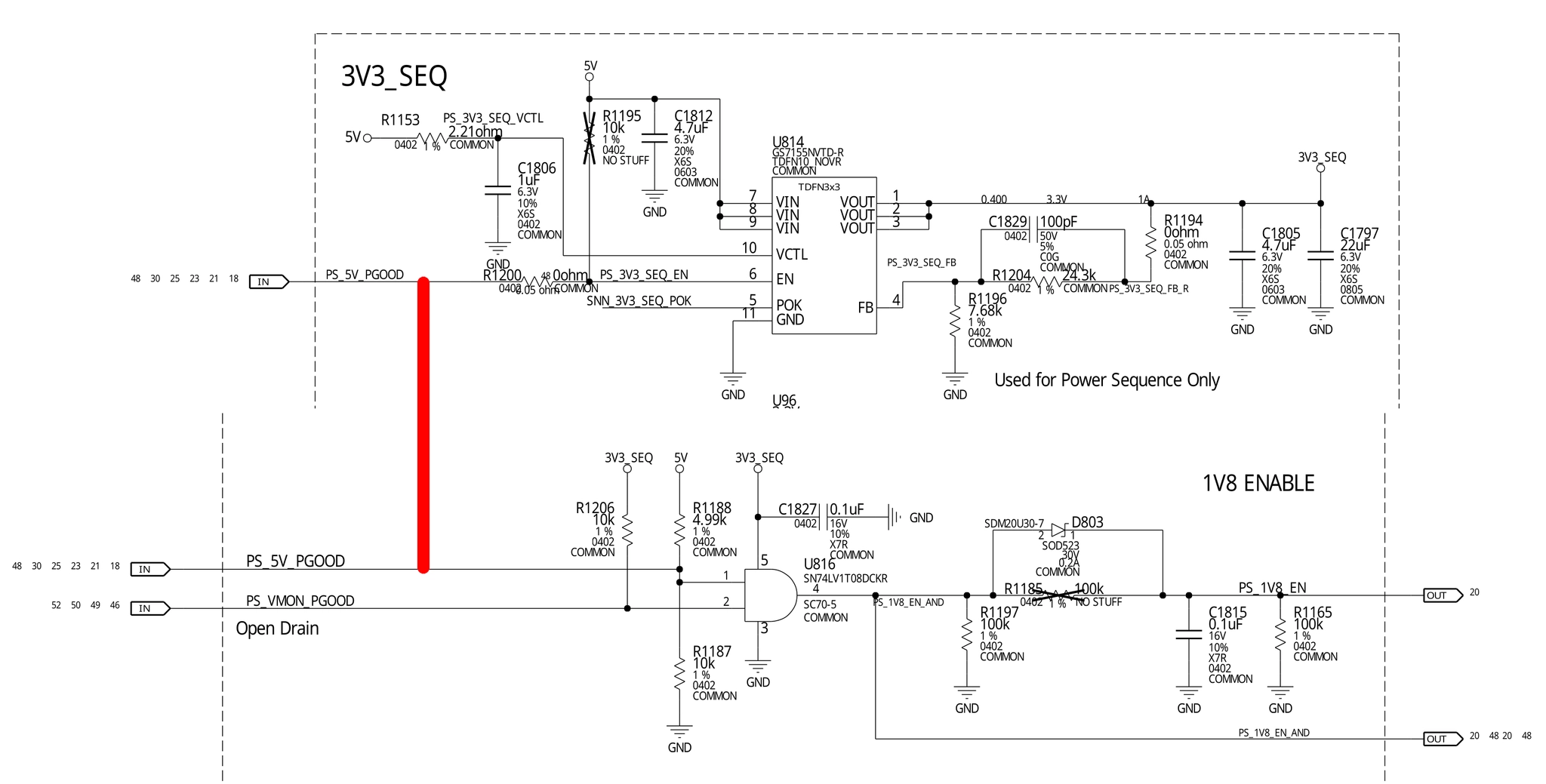
Power Tree
When a GPU can no longer be detected from PCIe, its on-board DC/DC power supplies are the first things to check.
Complex ASICs like a GPU usually contains multiple power domains for powering different subcircuits inside the chip. The circuit board itself also often needs several auxiliary logic voltages for the control and supporting circuitry. The malfunction of any of these voltage rails can prevent the GPU from starting up.
Helpfully, the first page of the Nvidia Tesla A100 schematics contains a power tree overview.
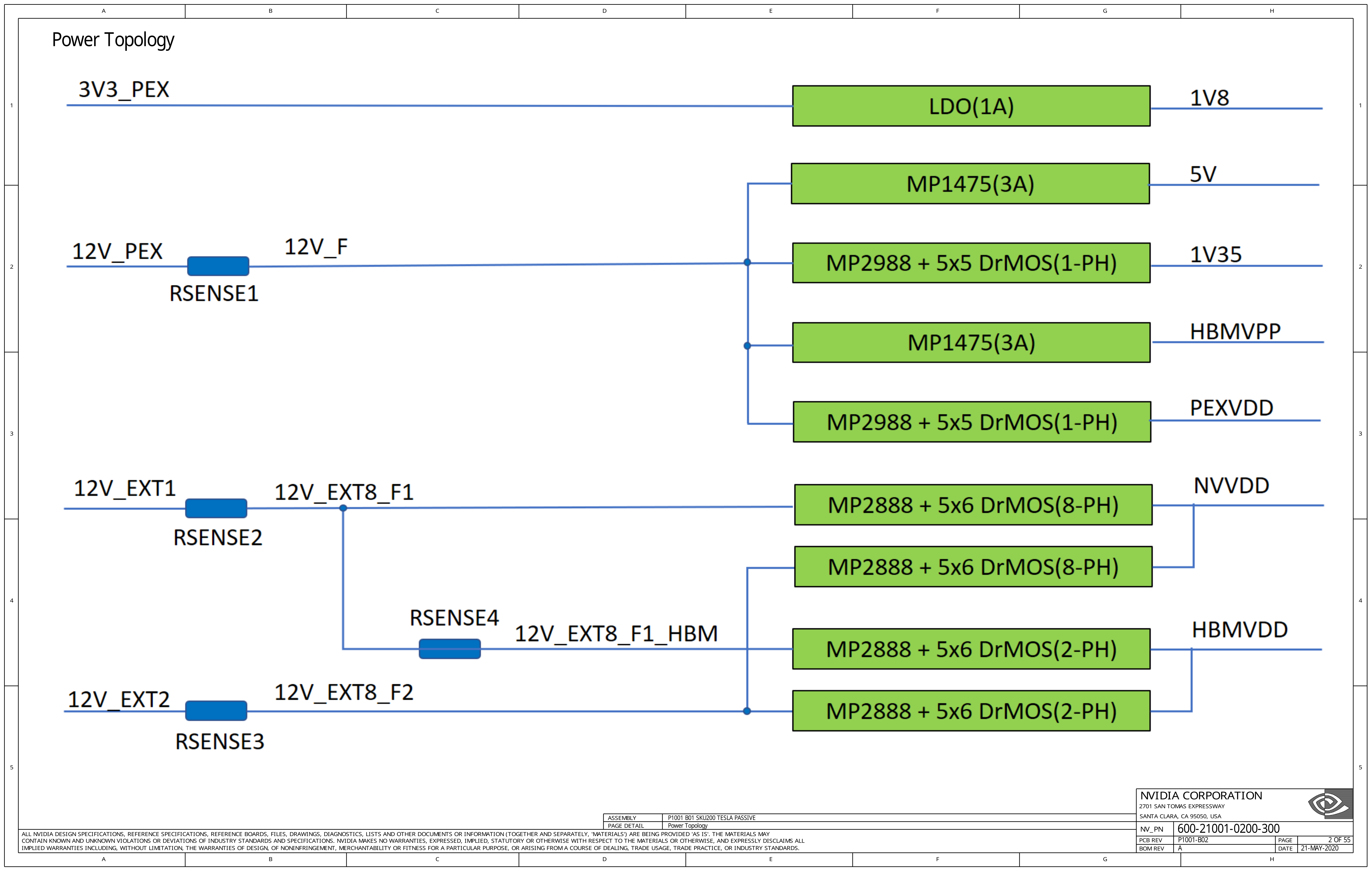
The PCB accepts four power inputs:
-
3V3_PEXis provided by the PCI Express (PEX) slot and is stepped down to 1.8 V for use by auxiliary control circuits using a 1.8 V Low-Dropout Linear Regulator (LDO). -
12V_PEXis provided by the PCI Express slot and is stepped down-
To 5 V via a DC/DC buck converter, the MP1475.
-
To 1.35 V via an MP2988 DC/DC controller (PWM controller), with one phase output to drive DrMOS switching transistors.
-
To
HBMVPP(2.5 V) via a DC/DC buck converter, another MP1475. This voltage is hooked into the GA100 silicon, but the power supply circuit is significantly simpler compared to the multi-phaseHBMVDDpower rail, so I suspect it’s used to power the memory controller itself. -
To
PEXVDDvia an MP2988 DC/DC controller, with one phase output to drive DrMOS switching transistors.PEXVDDbelongs to the I/O power domain for PCIe signaling.
-
-
12V_EXT1is provided by the first external 12 V power connector, which is used to derive the 1.0 V core voltage (NVVDD) and HBM memory voltage (HBMVDD) via the MP2988 DC/DC controller, which in turn drives DrMOS switching transistors using multiple phases.12V_EXT2serves the same purpose, but powers another group of power supply to provideHBMVDDandNVVDD. On the CMP 170HX and Tesla A100, both connectors are physically combined into a 8-pin CPU power connector, but one can still see two inputs when an adapter cable is used.
Initial Check
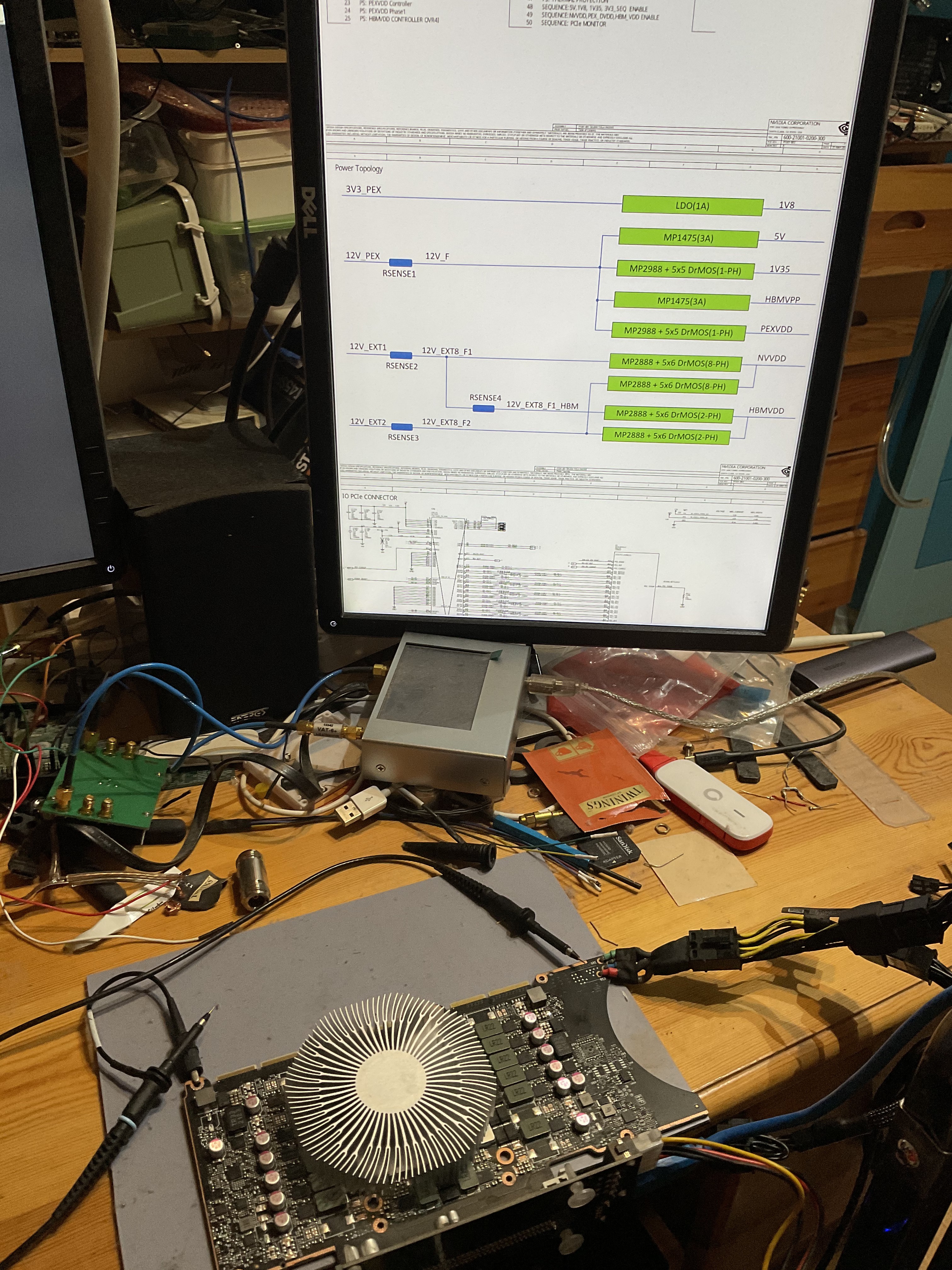
With the power tree in mind, it’s time for some basic checks for the voltage rails.
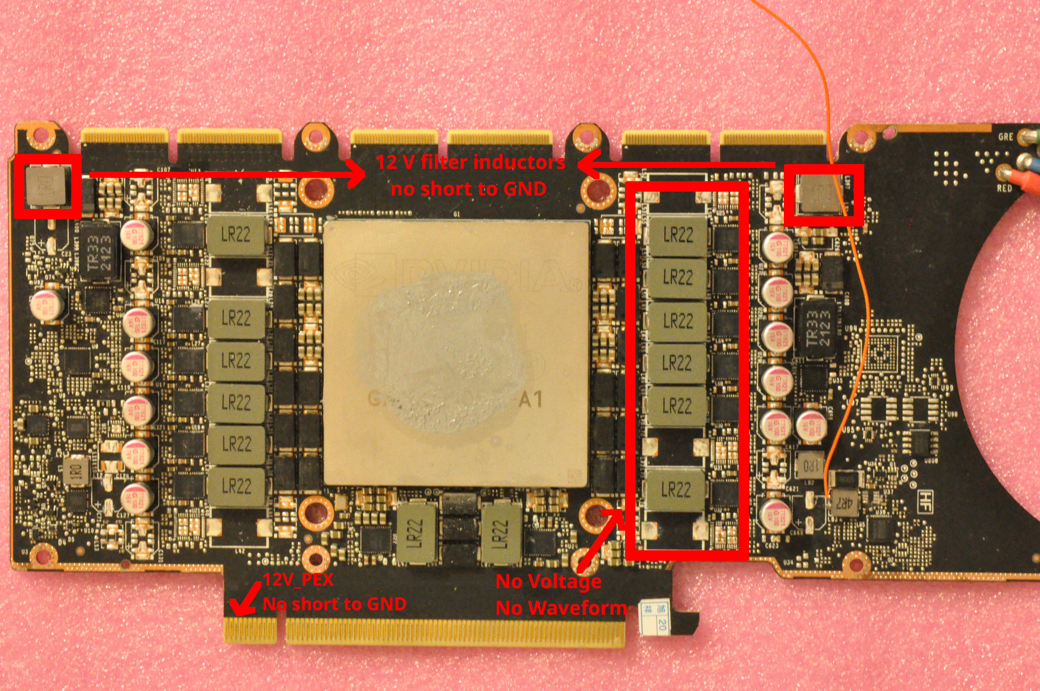
I measured the resistance from both 12 V external input filter inductors to ground, and found both have high impedance. I also measured the resistance from the left side of the PCIe connector to ground (which is the slot 12 V input), and also found no short circuit. Furthermore, after powering the card on and probing the output inductor on the right side of the core, I found none of them had any voltage output or switching waveforms.
This strongly suggests that a problem exists within the GPU’s power-on sequencing. Likely, a needed logic voltage is missing or entered protection due to a fault, preventing their downstream circuits from being enabled, including Vcore.
Power-On Sequencing
In circuit boards with multiple voltage rails, to avoid running the chips into an invalid state because some voltages are ready while others are not, or damaging circuit components due to backfeeding issues, power must be applied stage by stage from the upstream to the downstream in the correct order. This process is called Power-On Sequencing, controlled by a combination of Power Good and ENABLE signals, voltage comparators, logic gates, discrete transistors, and microcontrollers. A missing voltage or signal would prevent the GPU ASIC from powering on for protection - a good design should do that. The roles of each power rail and their timing during power-on sequencing is crucial for any board repair.
Therefore, the next step of the investigation was understanding how power-on sequencing works, which was answered in schematics on page 48.
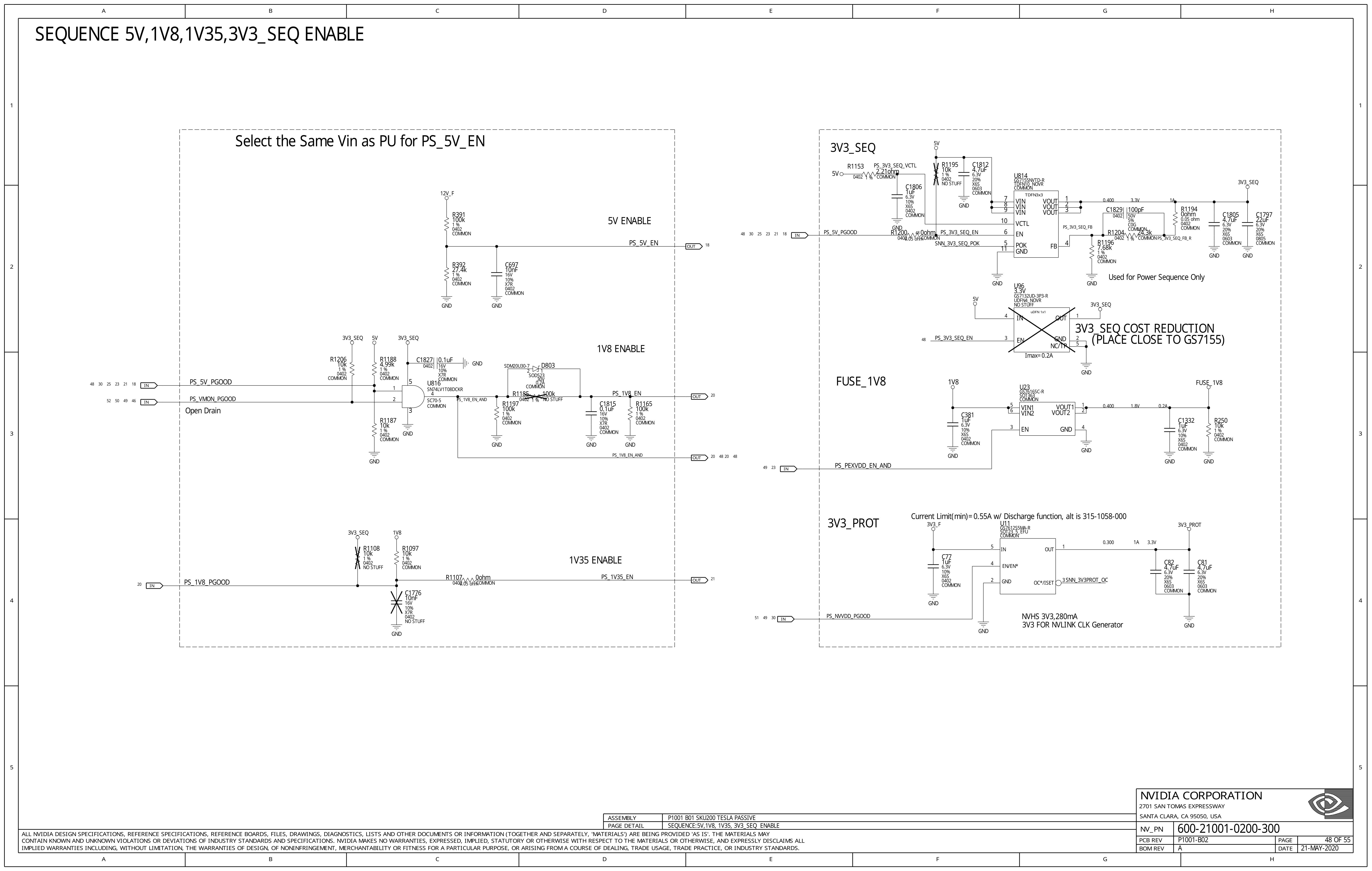
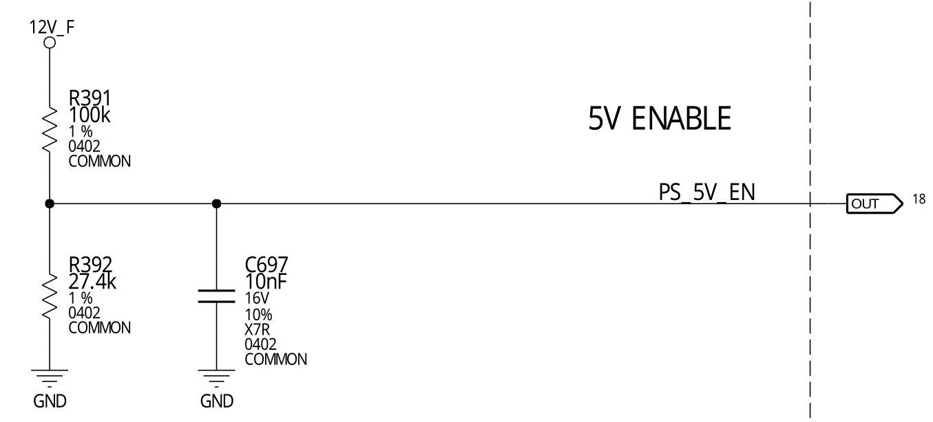
From this schematics, it’s obvious that the power-on sequencing is triggered by
applying 12 V input power (12V_F, F stands for “filtered”, which means it’s
the downstream of the input LC filter). This action causes the resistive
divider R391/R392 to produce a 2.5 V output at an appropriate logic level, which
is then used as the enabling signal 5V_PS_EN to start the 5 V DC/DC converter.
There’s also a tiny 10 nF capacitor to de-glitch this signal.
5 V supply
The 5V_PS_EN signal is then received by MP1475DJ on page 18, it’s
an adjustable DC/DC converter made by Monolithic Power Systems
with a really basic circuit topology - 12 V input, a switching node
SW driven by an internal switching transistor to generate a
switching waveform, which is then filtered by an output inductor
and output capacitor to generate a reduced voltage. The output
voltage is sampled via a voltage divider and fed back into the FB
pin for closed-loop control.
Although I’ve never used the exact chip, it’s a fact that almost every microcontroller circuit board I’ve previously designed contained a basic buck converter like this one. There is no complex controller-transistor combinations and no multi-phase switching, since it’s only a simple auxiliary voltage for powering the logic chips, not the GPU.
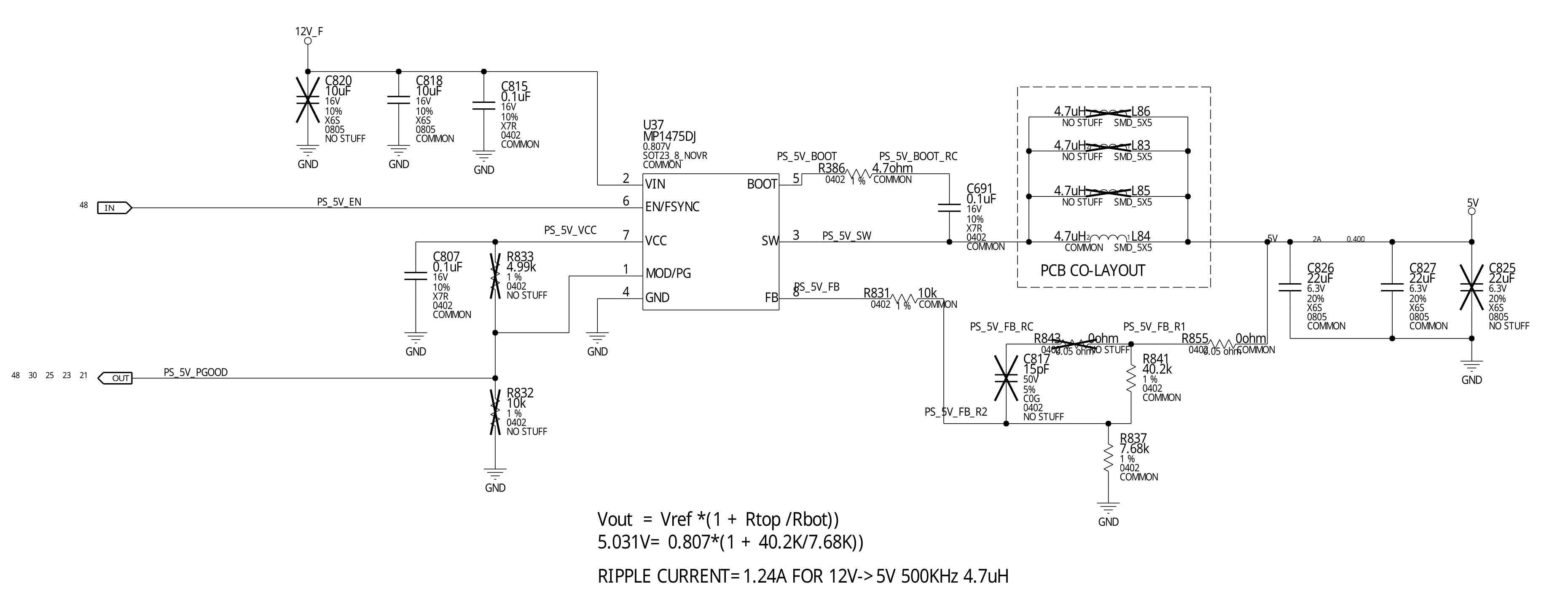
After pinpointing the physical location of the DC/DC converter and
measuring its switching node, I immediately found the first problem -
the 5 V DC/DC converter was refusing to start. At the switching node
SW, there was a momentary pulse that lasted for dozens of nanoseconds
before it stopped. The IC would then retry again after dozens of
microseconds but fail to start again, and this cycle repeats. This either
suggested the
existence of a short circuit in the 5 V rail, causing the power chip
to enter hiccup-mode short-circuit protection - or implied the DC/DC
converter was faulty.
To allow measuring its surrounding circuits at each pin individually with a multimeter without the interference from the potential faulty chip, I desoldered the MP1475DJ IC using my hot air gun. I also soldered a jumper wire to its output inductor for injecting an external 5 V voltage from my benchtop power supply to see whether overcurrent exists with a known-good 5 V source.
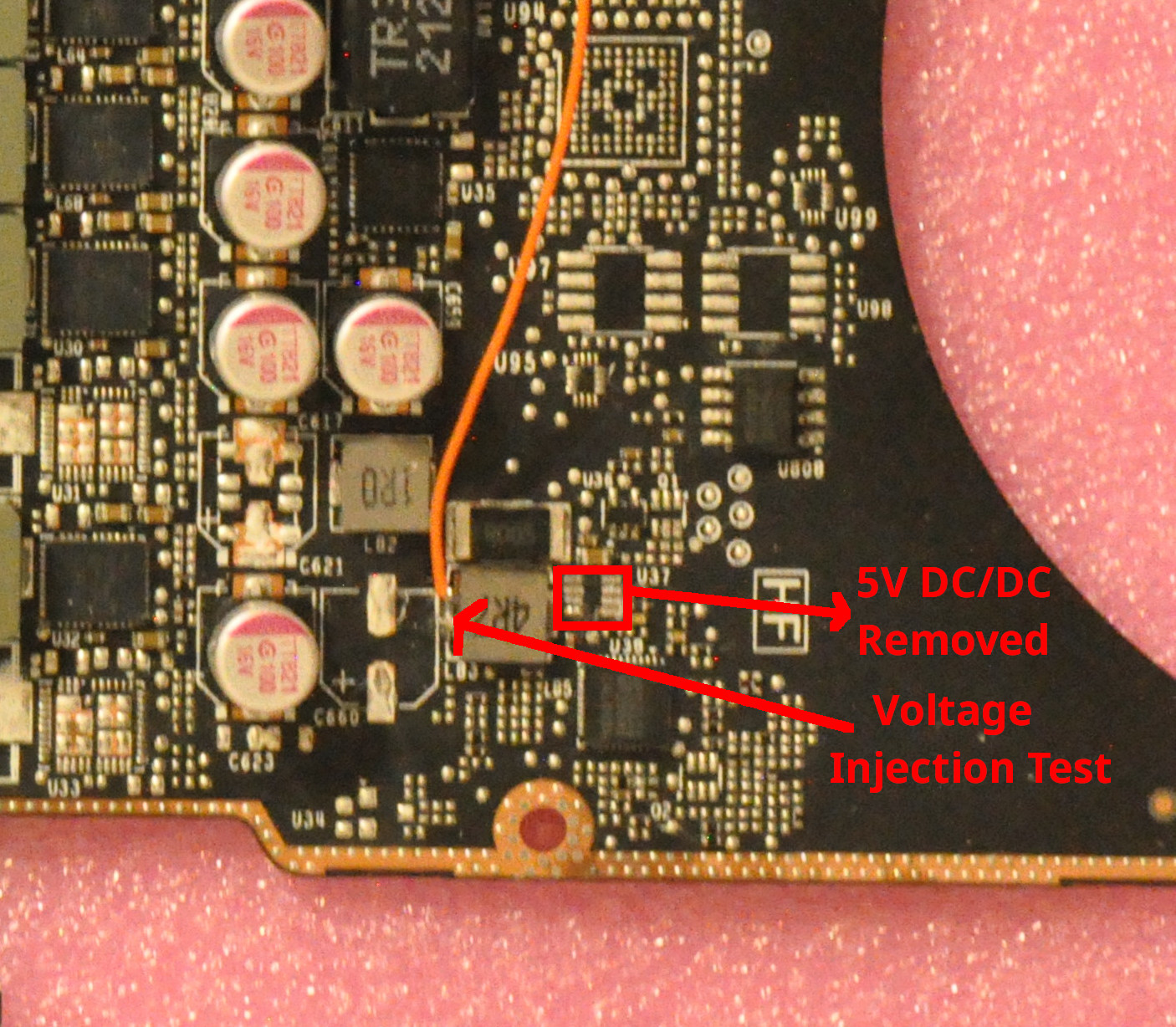
Voltage injection showed no short circuit. However, I discovered that the resistance from the empty footprint Pin 1 (Power Good signal) to ground was 5 Ω, this is not good! A short circuit on this signal meant the 5 V DC/DC chip would have a short circuit on its output pin whenever the power supply is ready - explaining why it was unable to start. It also meant that nothing downstream can start anymore since nothing could see the 5 V Power Good signal coming out anymore. Worse, it meant one of the users of this signal downstream has an internal short circuit at its input.
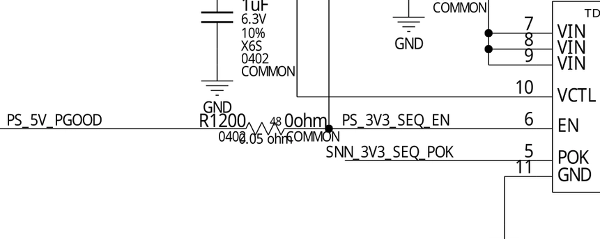
Hence, the next step was to investigate where the signal PS_5V_PGOOD
went.
PS_5V_PGOOD short circuit
After chasing for the net label PS_5V_PGOOD across the entire schematics,
I found the vast majority of its users are the logic chips, SN74LV1T08.
This chip is one of the modern remakes of the classic 74xx logic gates,
providing a 2-input AND gate with level shifting for controlling power
sequencing elsewhere, including PEXVDD, NVVDD, 1V35, and 1V8.
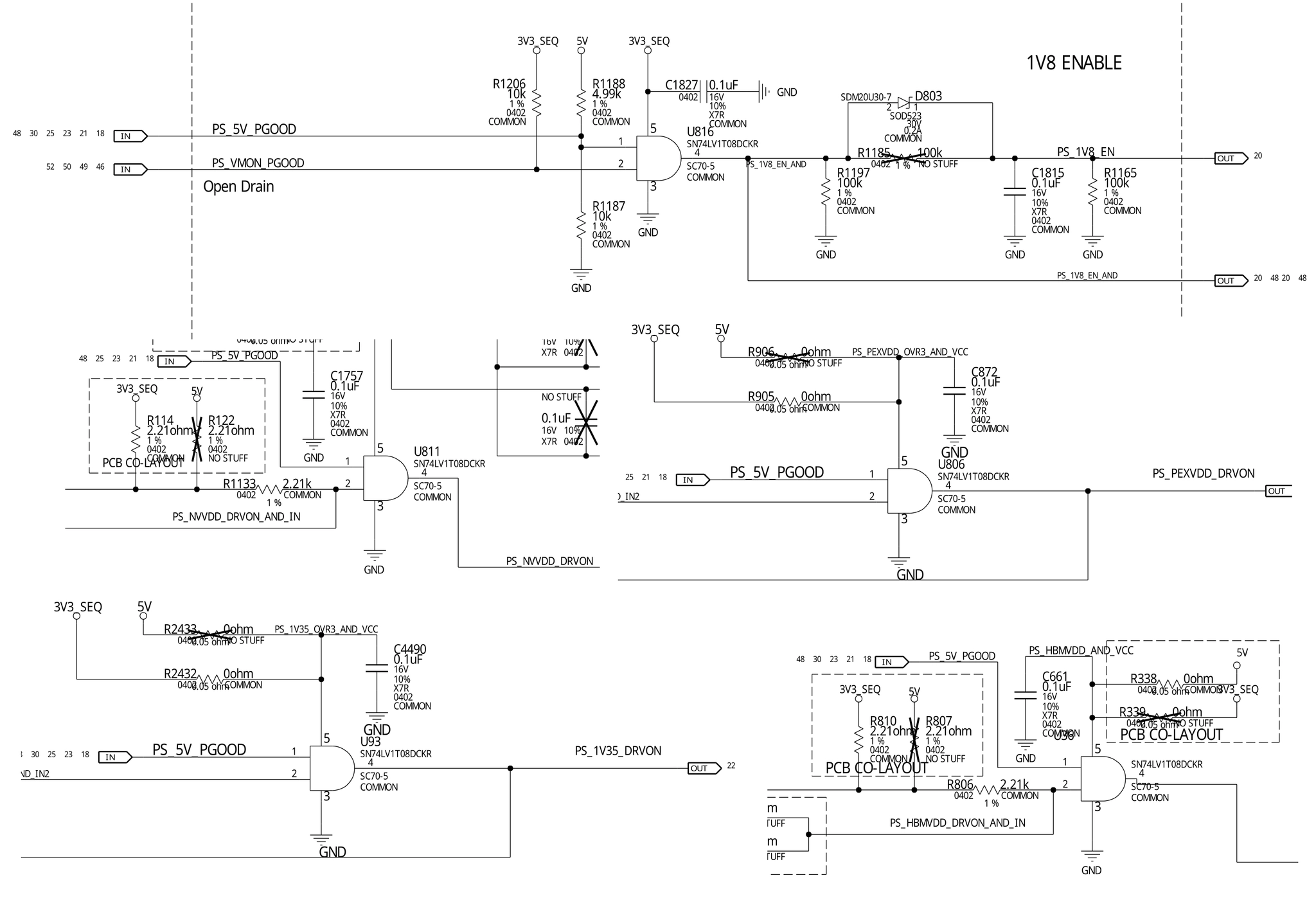
If any of these 74-logic chips is shorted, isolating the fault would be a painstaking task to desolder and check them one by one.
One of these things is not like the other, though. the 5V Power Good
signal is also used to enable the 5 V to 3.3 V Low-Dropout Regulator (LDO)
to produce 3V3_SEQ, an auxiliary 3.3 V logic voltage, which is only
used for continuing the power sequencing after 5 V (including powering
these 74 logic chips).
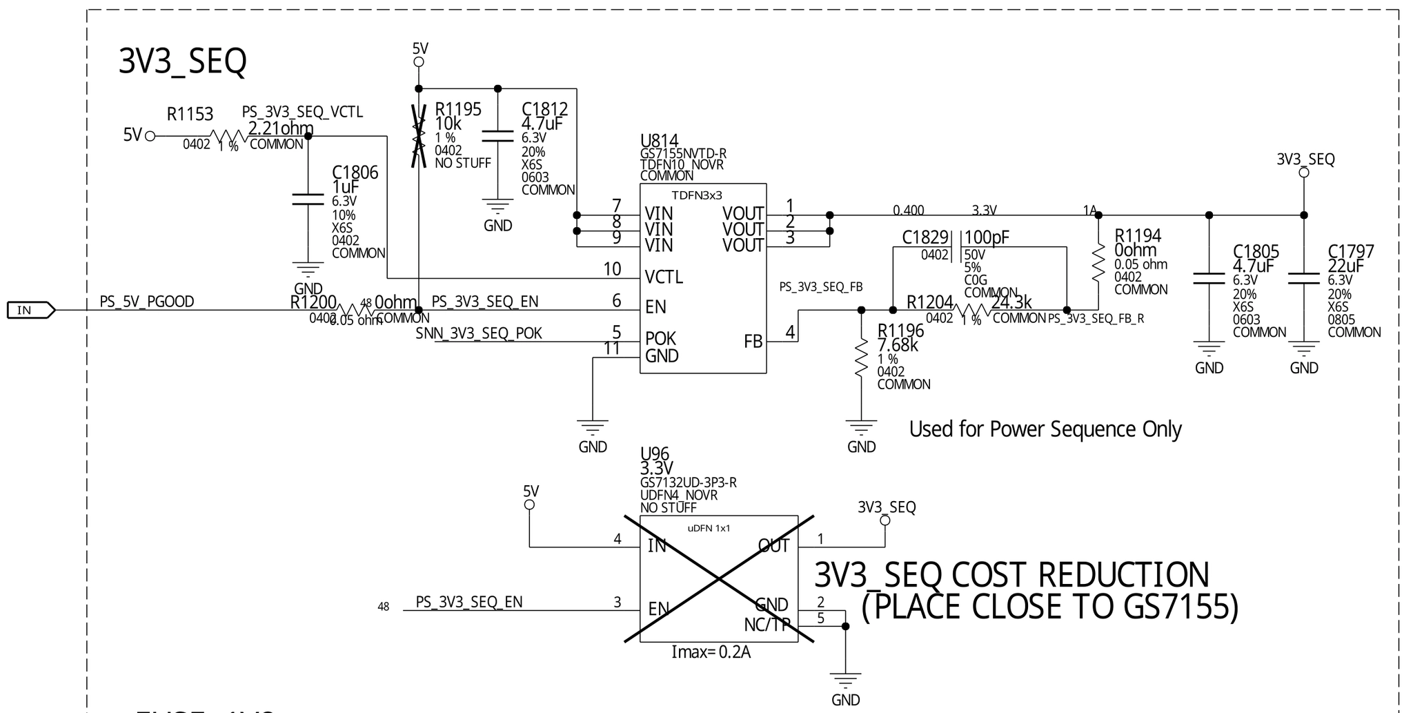
Conveniently, there’s a 0-ohm resistor jumper R1200 between the PS_5V_PGOOD
input and the ENABLE pin of the 3.3 V LDO. Thus, removing R1200 became
a no-brainer.
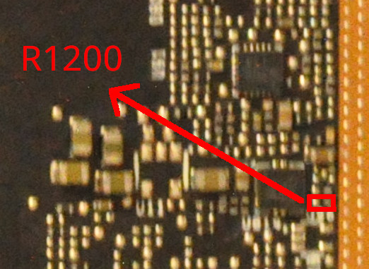
After I pushed away this 0402 resistor R1200 with a blob of molten
solder on the tip of my soldering iron, the short circuit at Pin 1
of MP1475DJ (in other words, PS_5V_PGOOD) has cleared - giving
confirmation that the GS7155NVTD LDO was dead due to an internal
short circuit.
5 V repair success!
When the problems were identified, I immediately ordered replacement chips for the MP1475DJ and GS7155NVTD. As soon as the MP1475DJs arrived, I resoldered a new one to the circuit board and applied power. Power-on tests showed the 5 V logic rail was successfully restored.
3.3 V supply
The next problem is replacing the GS7155NVTD.
The adjustable LDO chip GS7155NVTD is made by GSTEK. Although I’ve never used this chip or vendor before (apparently it’s specifically designed for powering Nvidia GPUs and its full datasheet is under NDA, although one can find the full datasheet of a similar model), but it’s also the most basic LDO circuit topology.
It accepts 5 V and generates 3.3 V by dropping the excess voltage away as heat using its internal series pass transistor. The output voltage is sampled by a resistive divider into the feedback pin for closed-loop control, voltage is adjustable by using different divider ratio. There’s also a capacitor across a feedback resistor, likely for frequency compensation of its control loop to improve its transient response performance - usually one just copies these components based on the manufacturer’s recommendations from the datasheet.
Using a hot-air gun, I quickly replaced the IC, but it was risky to power the board back on at this point. This chip uses the Quad No-Lead (QFN) package which is tricky to solder properly by hand. One needs to pre-tin the chip with solder, pre-tin the circuit board footprint with solder, then heat the PCB with a hot air gun. An inexperienced repair tech (like me) can easily create a cold solder joint, which is no joke.
If the feedback pin of the chip is open, from the perspective of the LDO, it would see a constant output undervoltage, and the LDO would put the maximum voltage on its output in an attempt to boost the output voltage. In reality, this causes the output voltage to shoot up to the max and creating full 5 V on the 3.3 V rail, thus blowing up almost all the 3.3 V logic chips with disastrous results. Therefore, I came up with an impoverished plan to distinguish a good and a bad LDO: I replaced the 7.68 kΩ feedback resistor at the bottom with a 20 kΩ resistor to temporarily reprogram the LDO’s output voltage from 3.3 V to 1.8 V, then I injected 3.3 V on the 5 V rail.
In the first attempt, I found the LDO couldn’t output any voltage - oh no… Circuit boards for computer motherboards and graphics cards contain many layers of power and ground planes, making them act as an excellent heatsink and a nightmare to repair. This is already sometimes a problem on my 4-layer PCBs, but modern computer cards often contain 8 to 12 layers of PCB to satisfy their high-speed signaling needs. On this card, I found I needed to set my hot-air gun to 420 degrees Celsius and to heat the area for 2 minutes before I was able to remove any chip. I really did not want to stress the circuit board further and risk lifting the copper pads or traces off the board with another round of hot-air gun torture (this is also why a pre-heater is needed for any serious BGA rework…)
Suddenly I realized that the ENABLE signal for the LDO was
missing. After bridging the LDO’s ENABLE signal to 3.3 V,
luckily, 1.8 V immediately appeared on the output side of the
LDO, bingo! This test showed that the LDO could correctly output a
regulated 1.8 V voltage, proving its correct operation.
Enabling ENABLE
After this test, I reinstalled the 7.68 kΩ feedback resistor to reprogram the LDO from 1.8 V back to 3.3 V. Now it’s the moment of truth, I replugged the card back into the test bench and powered it on…
Unfortunately, the 3.3 V rail has no output, the symptom was identical to the previous case of a missing ENABLE signal. What was going on?
Upon further probing with a multimeter, I found the left solder pad and right solder pad of the 0-ohm jumper R1200 was a short circuit - indeed, a close inspection under the microscope showed that there’s a trace directly bridging the pads! It must have been the case that the PCB designers wanted to remove the useless jumper R1200 (perhaps it’s a common point of failure), hence a direct copper trace was used to bypass R1200. But for some manufacturing reason, possibly to avoid reprogramming the pick-and-place machine or the automatic optical inspection machine, the now-useless resistor itself was kept as-is and not removed.
Hence, removing the resistor should not have isolated the original short
circuit inside the GS7155NVTD. Instead, in the process of removing R1200
or replacing other components, I may have accidentally damaged a via or
a trace on the circuit board, thus isolating the short circuit by breaking
the PCB itself. It’s also possible that the via or trace involved already
became fragile due to the previous short circuit. After breakage, the
enable signal GS7155NVTD became an isolated island unconnected to the
broader PS_5V_PGOOD net.
After the root cause was understood, solving the problem became trivial.
As I previously mentioned, the PS_5V_PGOOD net was used by many
SN74LV1T08 logic chips across the schematics for power sequencing.
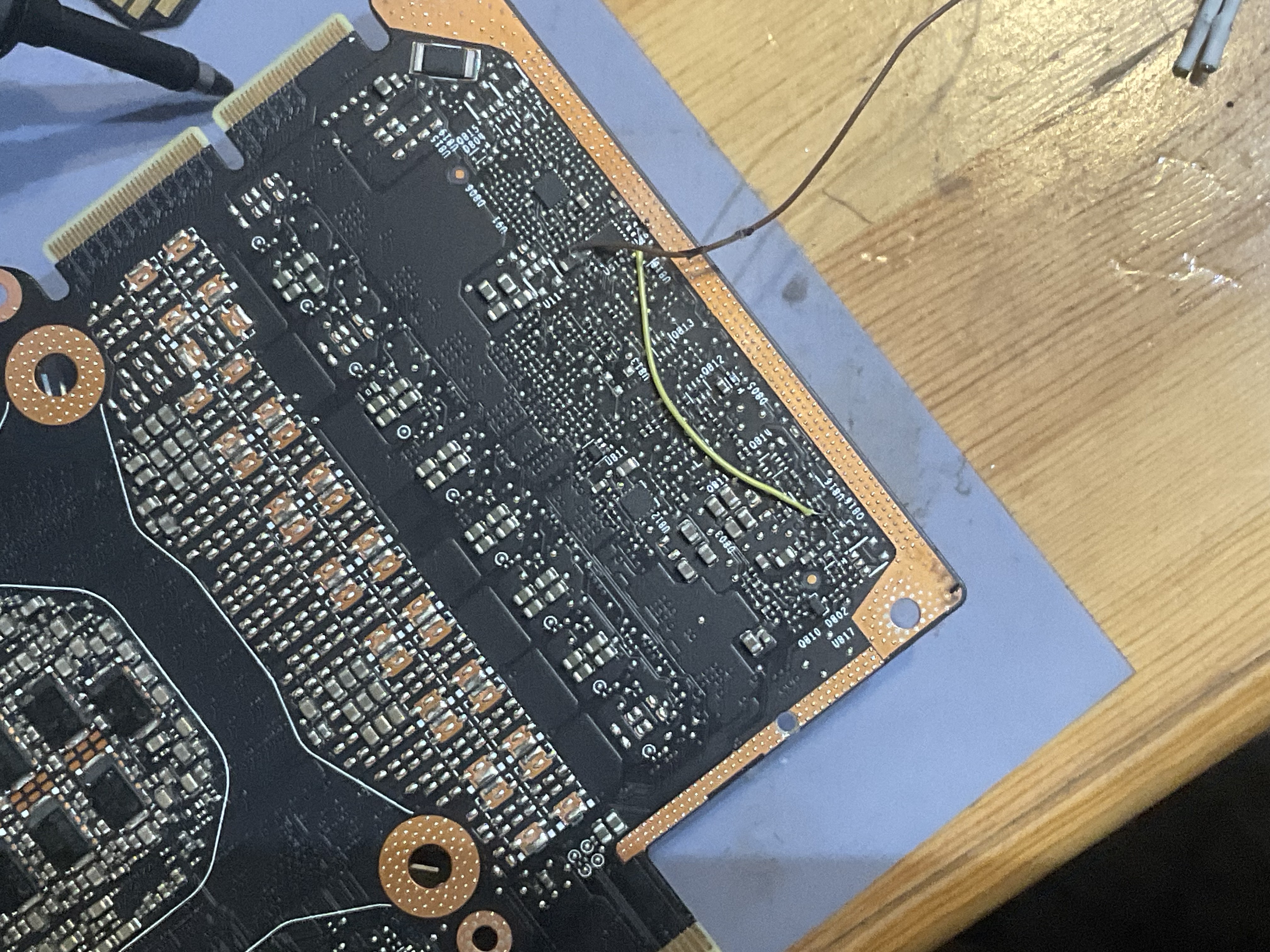
Thus, I decided to borrow this signal from U816 to GS7155NVTD using a jumper
wire.
Finally, I replugged the GPU into my test bench and reapplied power. 3.3 Vseq was back! I could see switching waveforms on the oscilloscope! 1.0 V Vcore (NVVDD) was back! PEXVDD was back! Finally, the GPU was redetected from PCIe, the GA100 is alive.
The photo above showed the use of a PVC-insulated AWG-30 wire-wrap wire - this was only used for a quick test, and is not recommended in an actual repair as it’s difficult to strip to wire to the correct length and to solder it without damaging its insulation - risking a short circuit due to wire movement. For the eventual repair, I used a thin enameled wire. Its heat-stripped insulation coating doesn’t suffer from this problem.